
Designing scan chains with specific parameter sensitivities to identify process defects

a scanning chain and sensitivity technology, applied in the direction of program control, instrumentation, semiconductor/solid-state device testing/measurement, etc., can solve the problems of scan chains that do not lend themselves to this approach, and achieve the effect of improving process defect monitoring, reducing chip surface area, and increasing diagnostic information

Inactive Publication Date: 2007-03-20
IBM CORP
View PDF16 Cites 25 Cited by
  • Summary
  • Abstract
  • Description
  • Claims
  • Application Information

AI Technical Summary

Benefits of technology

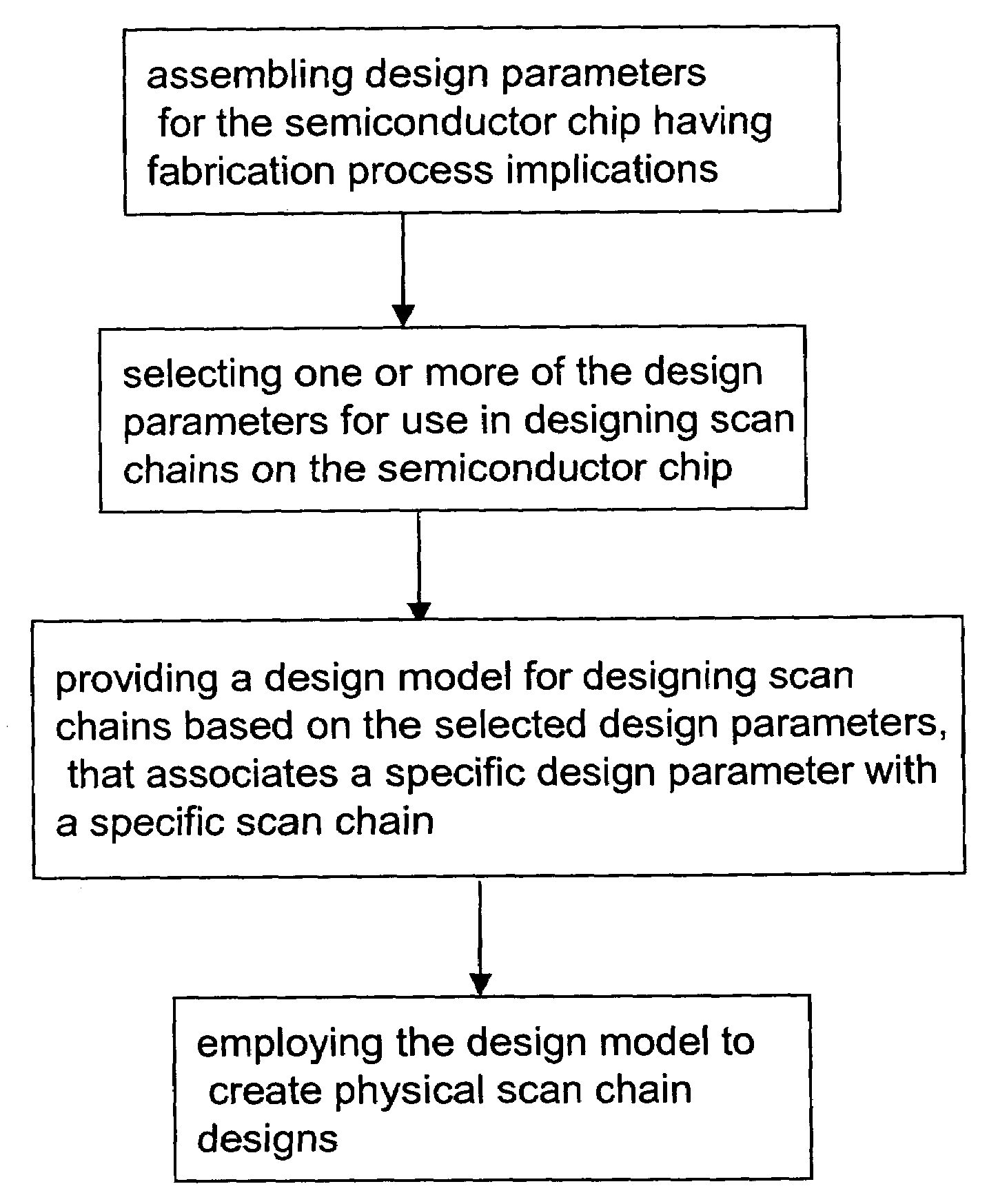
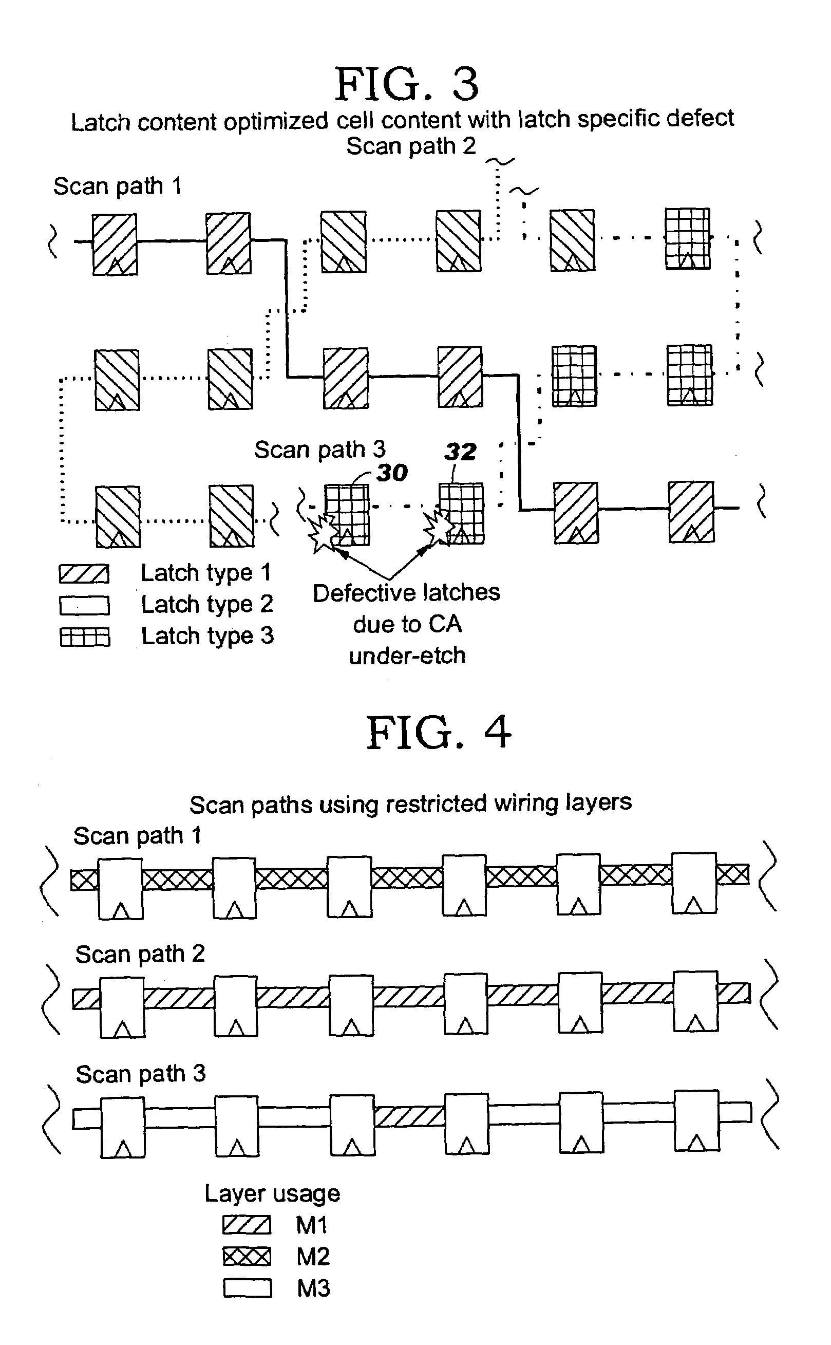
The present invention provides a scan chain design and test methodology that simultaneously provides desired test coverage and information on the state of specific process levels. The invention biases the composition of integrated circuit chip scan paths to function as on-product process monitors. The invention can design subsets of scan chains to have common latch cell usage and bias cell routing to given restricted metal layers for interconnects. The invention adds additional grouping constraints that bias scan chains to have common latch cell usage and bias cell routing. The invention increases the available diagnostic information that can be derived from scan fails during a scan chain test and improves process defect monitoring by using actual product chips and wafers. The invention requires a lesser number of kerf structures on chips and wafers, thus resulting in less area on chips and wafers being required to provide for the kerf structures. The invention is advantageous as it allows for testing after the wafers are diced and can be used to diagnose module final test problems, field returns, module level reliability issues, etc.

Problems solved by technology

However, some chip designs have scan chains that would not lend themselves to this approach.

Method used


Image

  • Designing scan chains with specific parameter sensitivities to identify process defects
  • Designing scan chains with specific parameter sensitivities to identify process defects
  • Designing scan chains with specific parameter sensitivities to identify process defects

Examples


Embodiment Construction

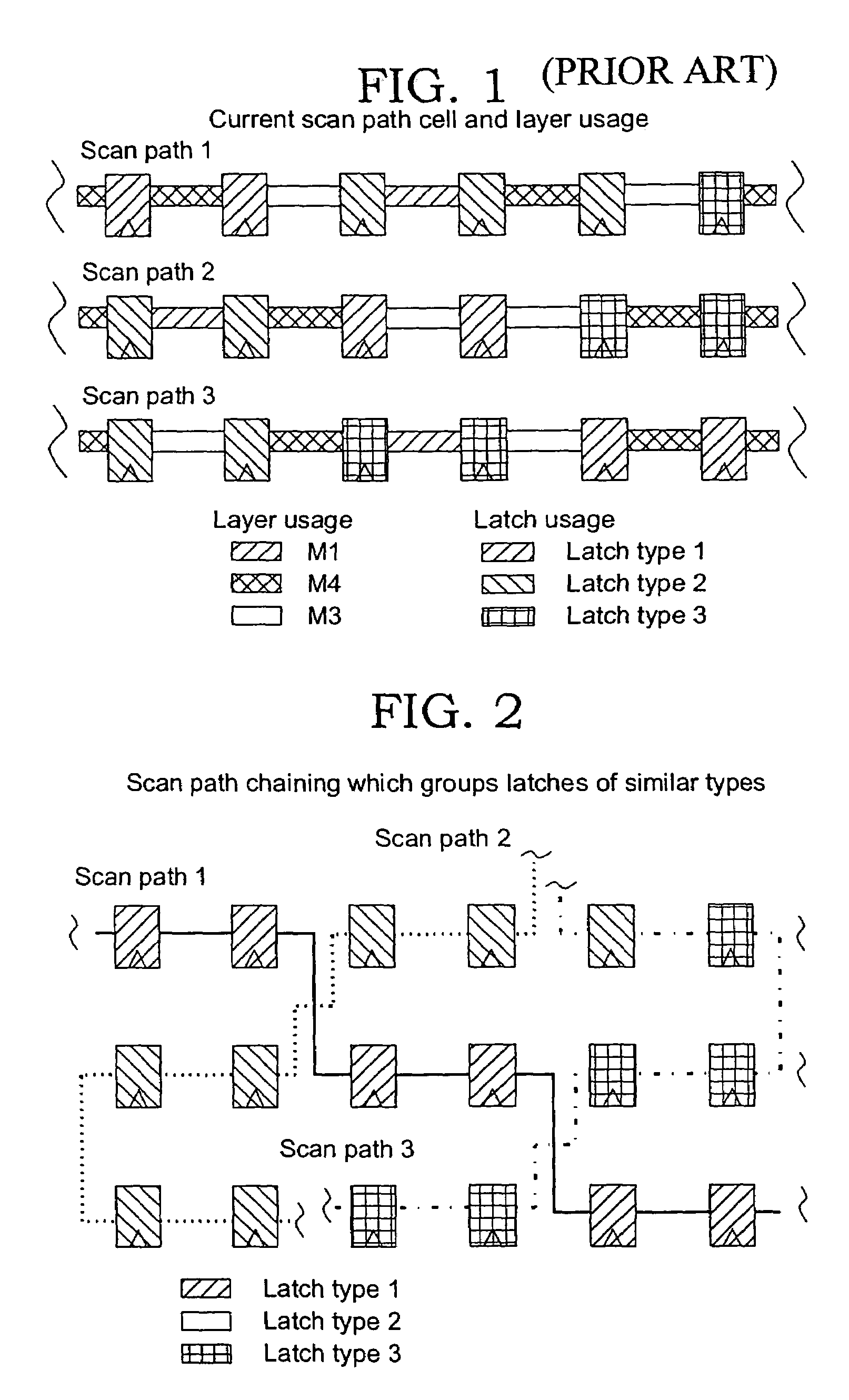
[0022]In the current state of the art, latches are wired together into scan chains to facilitate LSSD (level sensitive scan design) or other scan based testing. Latches in a design are gathered together to form scan chains based primarily upon physical design characteristics such as physical locality, voltage island affinity (the circuitry and components on a chip are frequently operated at several different voltage levels, and the various circuitry and components required to operate at a particular voltage level are frequently grouped together in one area of the chip), and scan chain length constraints.

[0023]FIG. 1 illustrates typical scan chains in the current state of the art as being composed of a mixture of cell / latch usage and layer usage. Scan chain / path 1 includes, proceeding from left to right, metal layer M4, latch type 1, metal layer M4, latch type 1, metal layer M3, latch type 2, metal layer M1, latch type 2, metal layer M4, latch type 2, metal layer M3, latch type 3, an...


PUM


Abstract

A method is disclosed for designing scan chains in an integrated circuit chip with specific parameter sensitivities to identify fabrication process defects causing test fails and chip yield loss. The composition of scan paths in the integrated circuit chip is biased to allow them to also function as on-product process monitors. The method adds grouping constraints that bias scan chains to have common latch cell usage where possible, and also biases cell routing to constrain scan chain routing to given restricted metal layers for interconnects. The method assembles a list of latch design parameters which are sensitive to process variation or integrity, and formulates a plan for scan chain design which determines the number and the length of scan chains. A model is formulated of scan chain design based upon current state of yield and process integrity, wherein certain latch designs having dominant sensitivities are chosen for specific ones of the scan chains on the chip. The model is provided as input parameters to a global placement and wiring program used to lay out the scan chains. Test data on the chip is then analyzed to determine and isolate systematic yield problems denoted by attributes of a statistically significant failing population of a specific type of scan chain.

Description

BACKGROUND OF INVENTION[0001]1. Field of the Invention[0002]The present invention relates generally to a method for designing scan chains in an integrated circuit chip with specific parameter sensitivities to identify fabrication process defects causing test fails and chip yield loss. The subject invention biases the composition of the integrated circuit chip scan paths to allow them to also function as on-product process monitors, and adds grouping constraints that bias scan chains to have common latch cell usage where possible, and also biases inter-cell routing to constrain scan chain routing to given restricted metal layers for interconnects. The grouping of structures with similar process sensitivities into a scan chain allows scan chain fails during test to be more easily correlated back to a subset of fabrication process steps and related root causes.[0003]2. Discussion of the Prior Art[0004]The semiconductor industry places a premium on the ability of new technologies to inc...

Claims


Application Information

Patent Timeline
Patent Type & Authority Patents(United States)
IPC IPC(8): G06F17/50
CPCG01R31/31855G01R31/318586G06F17/5045H01L22/34H01L2924/0002H01L2924/00G06F30/30
Inventor ADKISSON, JAMES W.BAZAN, GREGCOHN, JOHN M.GRADY, MATTHEW S.HUISMAN, LEENDERT M.JAFFE, MARK D.NIGH, PHILLIP J.PASTEL, LEAH M. P.SOPCHAK, THOMAS G.SWEENOR, DAVID E.VALLETT, DAVID P.
Owner IBM CORP
Learn More