High spatial resolution non-contact temperature measurement

Inactive Publication Date: 2013-12-19
RENESSELAER POLYTECHNIC INST
View PDF4 Cites 9 Cited by
  • Summary
  • Abstract
  • Description
  • Claims
  • Application Information

AI Technical Summary

Benefits of technology

[0013]Embodiments of the subject invention advantageously allow for collection of thermal, topographical, and other SEM images simultaneously from the same field of view.
[0014]In addition, systems, methods, and computer-readable media of the subject invention are easily integrated with existing SEMs. The hardware setup can be identical or nearly identical to a typical SEM equipped with an EBSD detector.
[0015]Embodiments of the subject invention can add a new channel—the temperature signal—to t

Problems solved by technology

Experimental studies of the nano-scale thermal processes involved in such systems are not possible without high spatial resolution temperature measurement techniques.
This causes an associated heat diffusion delay, topography-related artifacts in the thermal images, artifacts resulting from heat exchange through the sides of the probe (rather than just the tip) and thus perturbs the original micro-scale temperature distribution of the sample.
Optical techniques, such as infrared thermography, fluorescence thermography, thermoreflectance microscopy, optical interferometry, and micro-Raman thermography, address these issues with optical non-contact temperature mapping, but the spatial resolution of optical thermometry is typically limited by the wavelength of the radiation employed and cannot reach the typical feature sizes of current nano-engine

Method used


Image

  • High spatial resolution non-contact temperature measurement
  • High spatial resolution non-contact temperature measurement
  • High spatial resolution non-contact temperature measurement

Examples


example 1

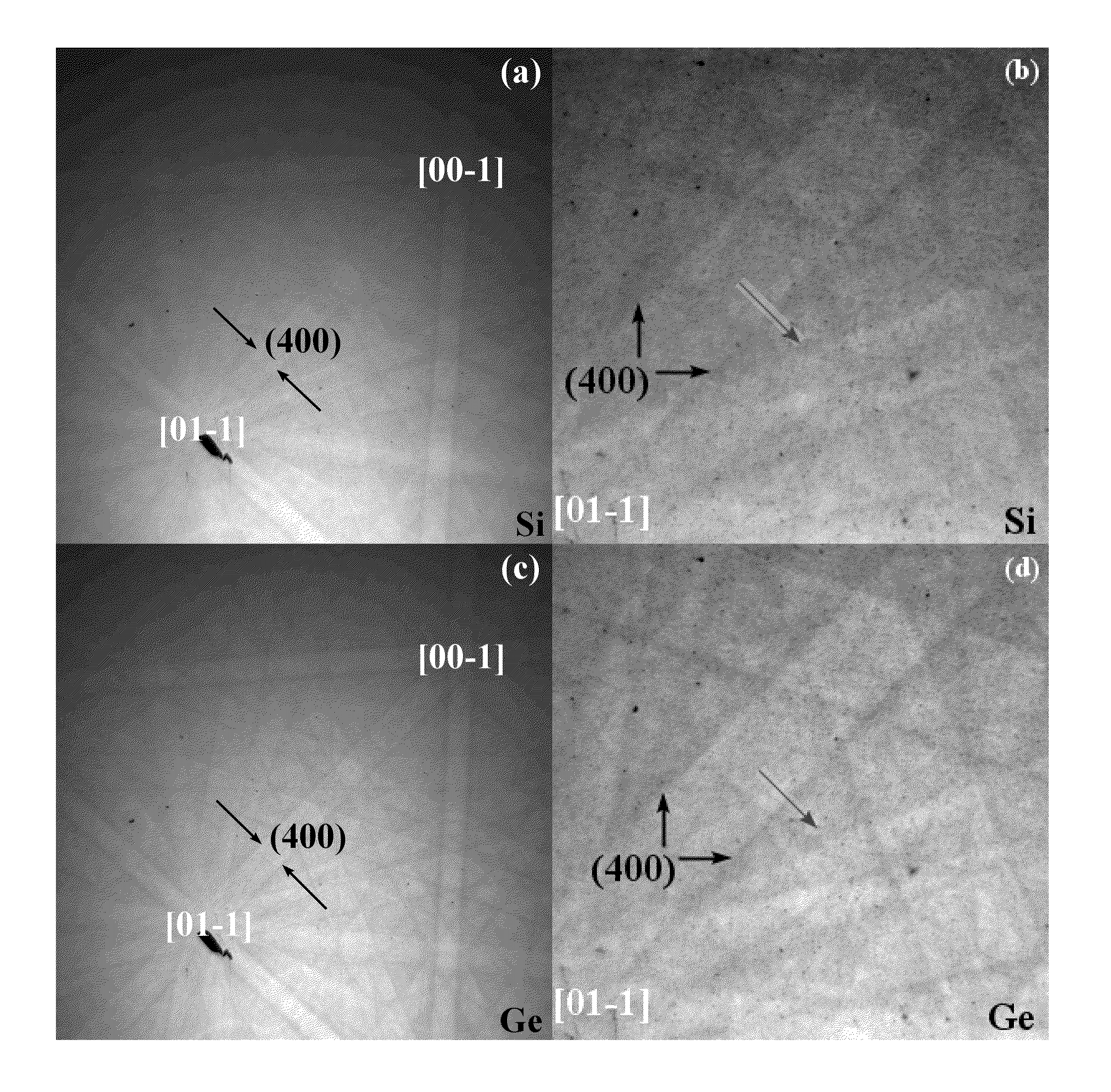
[0089]The EBSD data were obtained using a JEOL JEM 840 SEM with a custom-made heating stage from Ernest F. Fullam, Inc and an Oxford Instrument Nordlys II EBSD system. A two-step electron scattering process, consisting of incoherent scattering of incident beam electron followed by elastic and coherent scattering of these electrons, was performed to form EBSD Kikuchi patterns. The sample used for EBSD pattern collection at different temperatures was a single crystal {100} silicon wafer. The sample was mounted onto the hot stage in the SEM chamber using silver paint and the hot stage was tilted to 70° for EBSD collection. A K-type thermocouple was attached to the sample surface to provide an absolute calibration temperature. The hot stage and samples were then heated from room temperature to 400° C. and cooled back to room temperature very slowly to ensure that the temperature was close to uniform for each measurement. EBSD patterns at different temperatures were collected with the el...

example 2

[0112]In order to compare the effects of the above three material dependent factors experimentally, all other relevant factors should be precisely controlled. This requires materials for comparison which differ only in the above factors with all other parameters (especially those relevant to electron diffraction) the same or at least very close to each other. Single crystal Si and Ge {100} samples can be selected for these experiments due to the availability of pure and crysto-graphically perfect samples, their similar electron diffraction related material properties (e.g., the same crysto-graphic structure), but different B-factor sensitivities, atomic numbers, and lattice constants (i.e., the effects of the three factors to be compared).

[0113]ThSEM temperature measurements were performed on single crystal silicon {100} and germanium {100} samples. These samples were selected for due to the availability of pure and crysto-graphically perfect (or nearly perfect) samples, their simil...


PUM


Abstract

Advantageous systems, methods, and computer-readable media for temperature measurement of a sample, using new temperature measurement and mapping techniques, are provided. The technique employs a temperature sensitive electron signal in a scanning electron microscope (SEM) and provides both high spatial resolution and non-contact temperature measurement capabilities no existing technique can adequately combine. This technique thus adds a new capability—temperature measurement and mapping—to the collection of existing SEM capabilities.

Description

CROSS-REFERENCE TO RELATED APPLICATION[0001]The present application claims the benefit of U.S. Provisional Application Ser. No. 61 / 690,110, filed Jun. 19, 2012, which is hereby incorporated by reference herein in its entirety, including any figures, tables, and drawings.GOVERNMENT SUPPORT[0002]This invention was made with government support under Contract No. C090113 and Contract No. C080117 awarded by NYSTAR, and Contract No. 70NANB12H107 awarded by NIST. The government has certain rights in the invention.BACKGROUND[0003]Temperature measurement is important to studies of heat generation and transfer processes in a wide range of engineering systems. However, the feature sizes of many engineering systems, such as microelectronic, optoelectronic, and micromechanical systems, have been reduced down to length scales as small as tens of nanometers and continue to decrease. Experimental studies of the nano-scale thermal processes involved in such systems are not possible without high spat...

Claims


Application Information

Patent Timeline
IPC IPC(8): G01Q60/58
CPCG01Q60/58H01J37/244H01J37/28H01J2237/24585H01J2237/2804G01K9/00G01K11/30
Inventor WU, XIAOWEIHULL, ROBERT
Owner RENESSELAER POLYTECHNIC INST
Why Eureka
Try Eureka