Optical device

a technology of optical fibers and optical fibers, applied in the field of optical devices, can solve the problems of difficult use of pds in metal packages in combination with multiple-core optical fibers, and large size, and achieve the effect of reducing crosstalk

Inactive Publication Date: 2007-03-27
NGK INSULATORS LTD
View PDF93 Cites 9 Cited by
  • Summary
  • Abstract
  • Description
  • Claims
  • Application Information

AI Technical Summary

Benefits of technology

[0016]An object of the present invention is to provide an optical device which is capable of effectively reducing crosstalk even if reflected light is applied obliquely.
[0018]Of the gap between the principal surface of the second substrate and the optical element, a gap (first gap) between the active layer of the optical element and the principal surface of the second substrate and a gap (second gap) near and around the first gap have no light reflecting member such as of metal disposed therein. This arrangement is effective to suppress reflections at portions of the optical element and the principal surface of the second substrate which correspond to the first gap and the second gap. Even if the reflected light is applied obliquely, i.e., even if the reflected light is applied to the optical element at an angle of 10° or more with respect to the vertical direction, crosstalk can effectively be reduced.
[0022]In this manner, it is possible to suppress reflections at the interface between the optical element and the first and second gaps and also to spread in the reflected light in the first and second gaps, resulting in very small crosstalk.
[0025]Furthermore, of the gap between the principal surface of the second substrate and the optical element, a portion except the first gap and the second gap, i.e., a portion which does not affect the optical path of the reflected light, may have an electrode layer interposed therein. With such an arrangement, when the anisotropic conductive material is thermally compressed, electrodes, where an electrode pattern of Au or the like is raised, are brought into electric conduction with each other by the spherical polymer particles coated with the conductive material. However, in regions remote from the electrode layer, the spherical polymer particles are not held in contact with each other, and are interspersed at a low density. That is, the electrode layer disposed around the first gap and the second gap makes it possible to achieve a more preferable state.
[0026]As a consequence, the anisotropic conductive material can achieve both electric conduction between the optical element and the submount and scattering of the reflected light.
[0027]As described above, it is an object to cause light to be spread in the first gap and the second gap by either diffraction or scattering. Such an effect can be achieved if the length of the first gap and the second gap is large. The length should preferably be 20 μm or greater.

Problems solved by technology

Since the optical fibers need to be coupled to respective monitoring devices, the monitoring devices alone result in a considerable size.
However, it is difficult to use PDs in metal packages in combination with multiple-core optical fibers.
However, of reflected light from a certain channel, light that passes off the active layer of the PD array or passes through the active layer is reflected by the PD array or the mounting surface of the submount (the surface on which the PD array is mounted), and enters as stray light into another channel, tending to cause crosstalk.

Method used


Image

  • Optical device
  • Optical device
  • Optical device

Examples


first embodiment

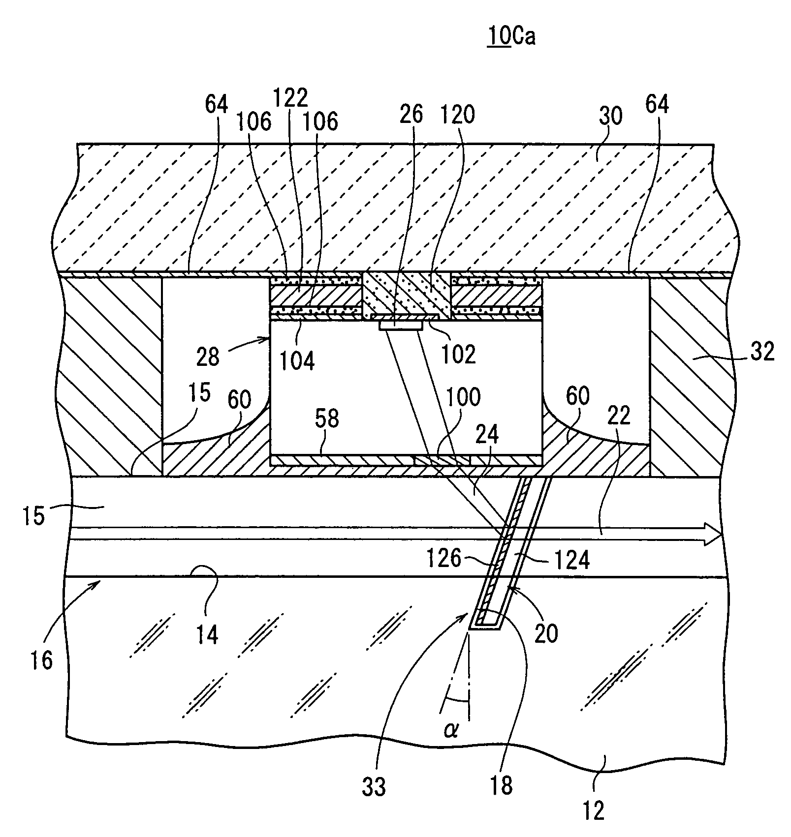
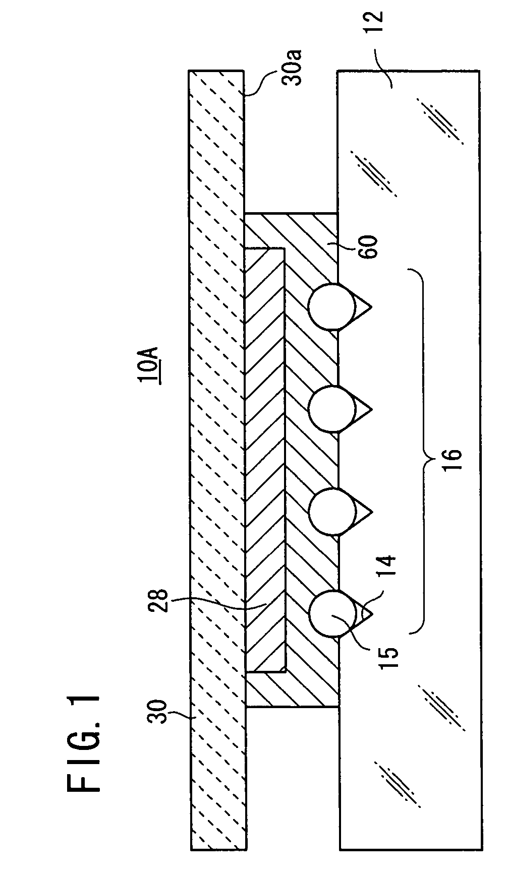
[0043]As shown in FIG. 1, an optical device 10A according to the present invention has a glass substrate 12, an optical fiber array 16 comprising a plurality of optical fibers 15 fixed in a plurality of V-shaped grooves 14 defined in the glass substrate 12, a PD (PhotoDiode) array 28 fixed by an adhesive layer 60 to an optical path of light (reflected light) 24 which is generated by at least a reflector, of signal light 22 passing through the optical fibers 15, for thereby detecting the reflected light 24, and a wiring board (submount) 30 on which the PD array 28 is mounted. The submount 30 has a mounting surface 30a for the PD array 28, disposed in confronting relation to the glass substrate 12.

[0044]In this embodiment, the optical fiber array 16 comprises a plurality of optical fibers 15, and “each of the optical fibers 15” means “each of the four optical fibers 15”. However, since even one optical fiber 15 can make up the optical fiber array 16, “each of the optical fibers” or “a...

second embodiment

[0058]An optical device 10B will be described below with reference to FIG. 4.

[0059]The optical device 10B according to the second embodiment is of substantially the same structure as the optical device 10A according to the first embodiment, but differs therefrom in that, as shown in FIG. 4, the first and second gaps 112, 114 are filled with an anisotropic conductive material 120 such as an ACP (anisotropic conductive paste), an ACF (anisotropic conductive film), or the like.

[0060]The anisotropic conductive material 120 contains therein interspersed spherical polymer particles coated with a conductive material such as gold or the like. The spherical polymer particles scatter the reflected light 24 to achieve desired scattering thereof. If the spherical polymer particles are so highly packed that they are held in contact with each other, then they tend to reflect the light largely. Therefore, even though the spherical polymer particles are partly held in contact with each other, they...

third embodiment

[0062]An optical device 10C will be described below with reference to FIG. 5. Those parts of the optical device 10C which correspond to those of the optical device 10B shown in FIG. 4 are denoted by identical reference characters and will not be described below.

[0063]The optical device 10C according to the third embodiment differs from the optical device 10B shown in FIG. 4 in that, as shown in FIG. 5, the PD array 28 is of a structure for detecting light applied to its reverse side.

[0064]The PD array 28 has a substrate 29 and as many active layers 26 as the number of channels on the substrate 29. The active layers 26 are disposed on a portion of the substrate 29 which is close to the submount 30 and the mounting surface 30a of the submount 30.

[0065]In the optical device 10C, a gold electrode pattern 104 on the PD array 28 and a gold electrode pattern 64 on the submount 30 are electrically connected to each other by a conductive layer 106 such as an ACP (anisotropic conductive past...


PUM


Abstract

An optical device comprises a PD array and a submount. Anode electrodes and cathode electrodes are disposed as a gold electrode pattern on a surface of the PD array facing the submount and a common cathode electrode and anode electrodes associated with respective channels are disposed as a gold electrode pattern on a mounting surface of the submount. The gold electrode pattern on the PD array and the gold electrode pattern on the submount are electrically connected to each other by a conductive layer. A gap between the PD array and the mounting surface of the submount includes a first gap corresponding to active layers and a second gap around the first gap, the first and second gaps comprising air.

Description

CROSS REFERENCE TO RELATED APPLICATIONS[0001]This application is a continuation-in-part of International Application No. PCT / JP2003 / 016345, having an international filing date of Dec. 19, 2003,which designated the United States, and is a continuation-in-part of U.S. application Ser. No. 10 / 732,203,filed Dec. 10, 2003 is now abandoned, which claims the benefit under 35 USC §119(e) of U.S. Provisional Application Ser. No. 601435,105,filed Dec. 20, 2002, the entireties of which are incorporated herein by reference.BACKGROUND OF THE INVENTION[0002]1. Field of the Invention[0003]The present invention relates to an optical device having an optical fiber array having one or more optical fibers, and more particularly to an optical device suitable for monitoring signal light while it is being propagated through an optical fiber.[0004]2. Description of the Related Art[0005]With the recent development of wavelength multiplex communications using fiber amplifiers, it has become customary to mon...

Claims


Application Information

Patent Timeline
Patent Type & Authority Patents(United States)
IPC IPC(8): G02B6/36G02B6/30G02B6/26G02B6/42
CPCG02B6/4214G02B6/4249G02B6/4246
Inventor FUKUYAMA, MASASHIIWASAKI, YASUNORIIDE, AKIYOSHI
Owner NGK INSULATORS LTD
Why Eureka
Try Eureka