Surface mount multi-channel optocoupler

a multi-channel optocoupler and surface mount technology, applied in the field of surface mount multi-channel optocouplers, can solve the problems of optocoupler packages b>10/b> that require an expensive and time-consuming overmolding process, and add to the time and expense of forming an optocoupler packag

Active Publication Date: 2007-03-27
SEMICON COMPONENTS IND LLC
View PDF93 Cites 91 Cited by
  • Summary
  • Abstract
  • Description
  • Claims
  • Application Information

AI Technical Summary

Problems solved by technology

For example, the optical receiver device cannot modify the operation of a circuit containing the optical emitter device.
For example, the optocoupler package 10 requires an expensive and time consuming overmolding process.
In addition to the overmolding process itself, mold material removal processes (e.g., dejunk and deflash processes) are used to remove excess molding compound, thus adding to the time and expense of forming an optocoupler package.
In addition, the tooling that is needed to create moldings of different “form factors” (e.g., 4, 6, or 8 pin packages) requires a significant capital investment.
The optocoupler package 10 is also prone to failure from thermal cycling.
The molding compound 18 and the optically transmissive medium 16 could potentially separate, thus resulting in a structurally weak package.
The stress can result in a broken or weakened lead frame 24.

Method used


Image

  • Surface mount multi-channel optocoupler
  • Surface mount multi-channel optocoupler
  • Surface mount multi-channel optocoupler

Examples


Embodiment Construction

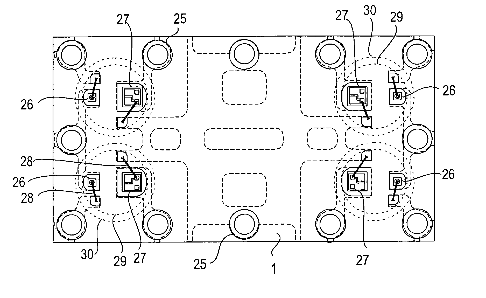
[0025]In embodiments of the invention, one or more optocouplers are on a single substrate that is formed from a leadframe and a molding compound. For example, there can be four optocouplers in a quad array on a single substrate. Each optocoupler can include an optical emitter (e.g., a light emitting diode) and an optical receiver (e.g., a photodiode). The spacing between the optical receiver and the optical emitter can be from about 0.3 mm to about 0.5 mm. Each optocoupler can be secured with an optically transmissive coupling gel and can be encapsulated with an opaque, highly reflective epoxy based polymer. The functional terminals for the optocouplers can be grouped and routed towards the periphery of the package so that a ball grid array layout is formed. The optical receivers, the optical emitters, and wire bond pads are arranged so that they will correspond to the terminals of the leadframe.

[0026]Logic devices such as control chips can also be on the leadframe-based substrate a...


PUM


Abstract

An optocoupler package is disclosed. The optocoupler package includes a substrate comprising a leadframe and a molding compound, and a plurality of optocouplers, each optocoupler including (i) an optical emitter, (ii) an optical receiver, (iii) and an optically transmissive medium disposed between the optical emitter and optical receiver, where the optical emitter and the optical receiver are electrically coupled to the leadframe.

Description

BACKGROUND OF THE INVENTION[0001]Optocouplers contain at least one optical emitter device which is optically coupled to an optical receiver device through an optically transmissive medium. This arrangement permits the passage of information from one electrical circuit that contains the optical emitter device to another electrical circuit that contains the optical receiver device. A high degree of electrical isolation is maintained between the two circuits. Because information is passed optically across an insulating gap, the transfer is one way. For example, the optical receiver device cannot modify the operation of a circuit containing the optical emitter device. This feature is important because, for example, the emitter may be driven by a low voltage circuit using a microprocessor or logic gates, while the output optical receiver device may be part of a high voltage DC or AC load circuit. The optical isolation also prevents damage to the input circuit caused by the relatively hos...

Claims


Application Information

Patent Timeline
Patent Type & Authority Patents(United States)
IPC IPC(8): H01L31/00G02B27/00A61B5/00G02B6/42H01J40/14
CPCG02B6/4201H01L2224/48091H01L2224/48247H01L2924/01046H01L2924/12041H01L2924/01079H01L2924/01078H01L2924/13055H01L2924/13091H01L2924/00014H01L2924/00
Inventor QUINONES, MARIA CLEMENS Y.JOSHI, RAJEEV
Owner SEMICON COMPONENTS IND LLC
Why Eureka
Try Eureka