

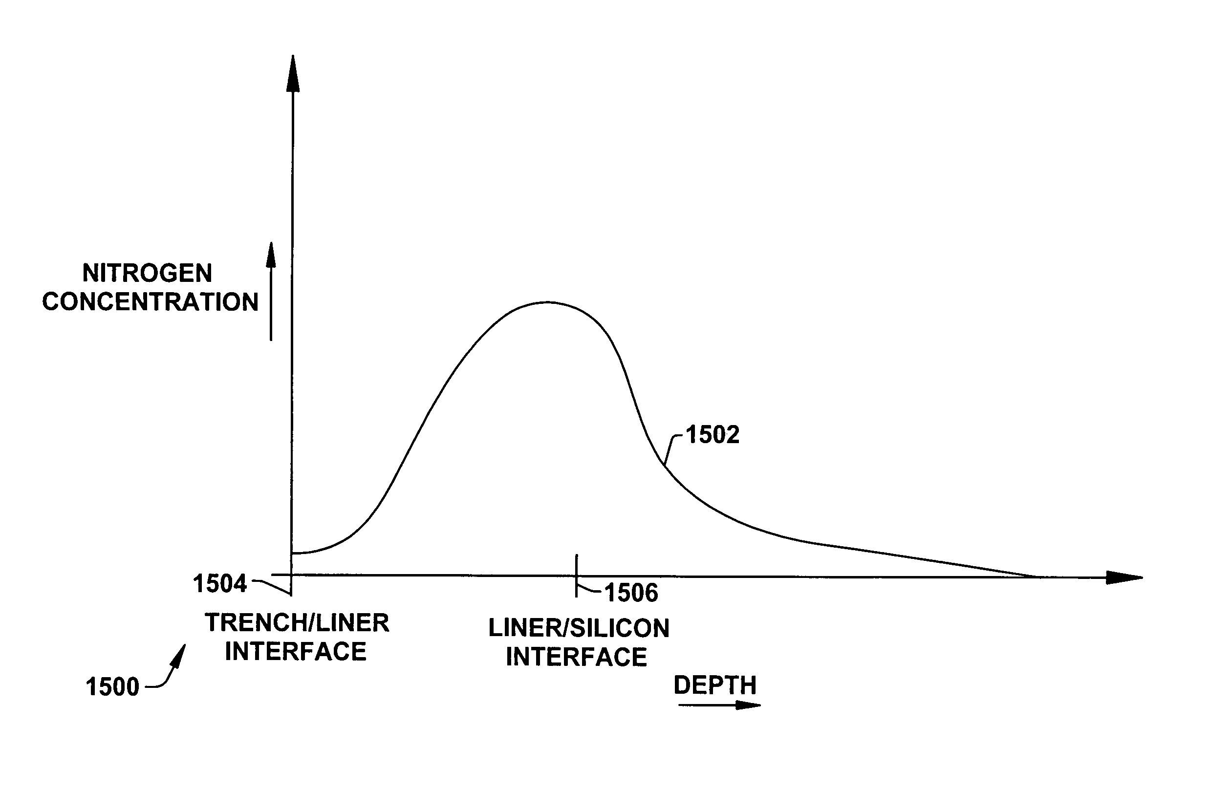
Nitridation of STI liner oxide for modulating inverse width effects in semiconductor devices
a technology of inverse width and nitridation, which is applied in the manufacture of semiconductor/solid-state devices, basic electric elements, electric devices, etc., can solve the problems of reducing the width of transistors, reducing the efficiency of semiconductor devices, so as to facilitate device operation and modulate the inverse width effect. , the effect of reducing the number of problems
- Summary
- Abstract
- Description
- Claims
- Application Information
AI Technical Summary
Benefits of technology
Problems solved by technology
Method used
Image

Examples
Embodiment Construction
[0021]The present invention will now be described with reference to the attached drawings, wherein like reference numerals are used to refer to like elements throughout. The invention relates to methods for forming isolation structures and trenches in semiconductor devices, in which the negative impacts of the INWE are eliminated or substantially mitigated without the addition of extra mask steps. In addition, the method according to one exemplary aspect of the invention advantageously operates to improve a balance or minimize an imbalance of the threshold voltage performance of NMOS and PMOS transistors.
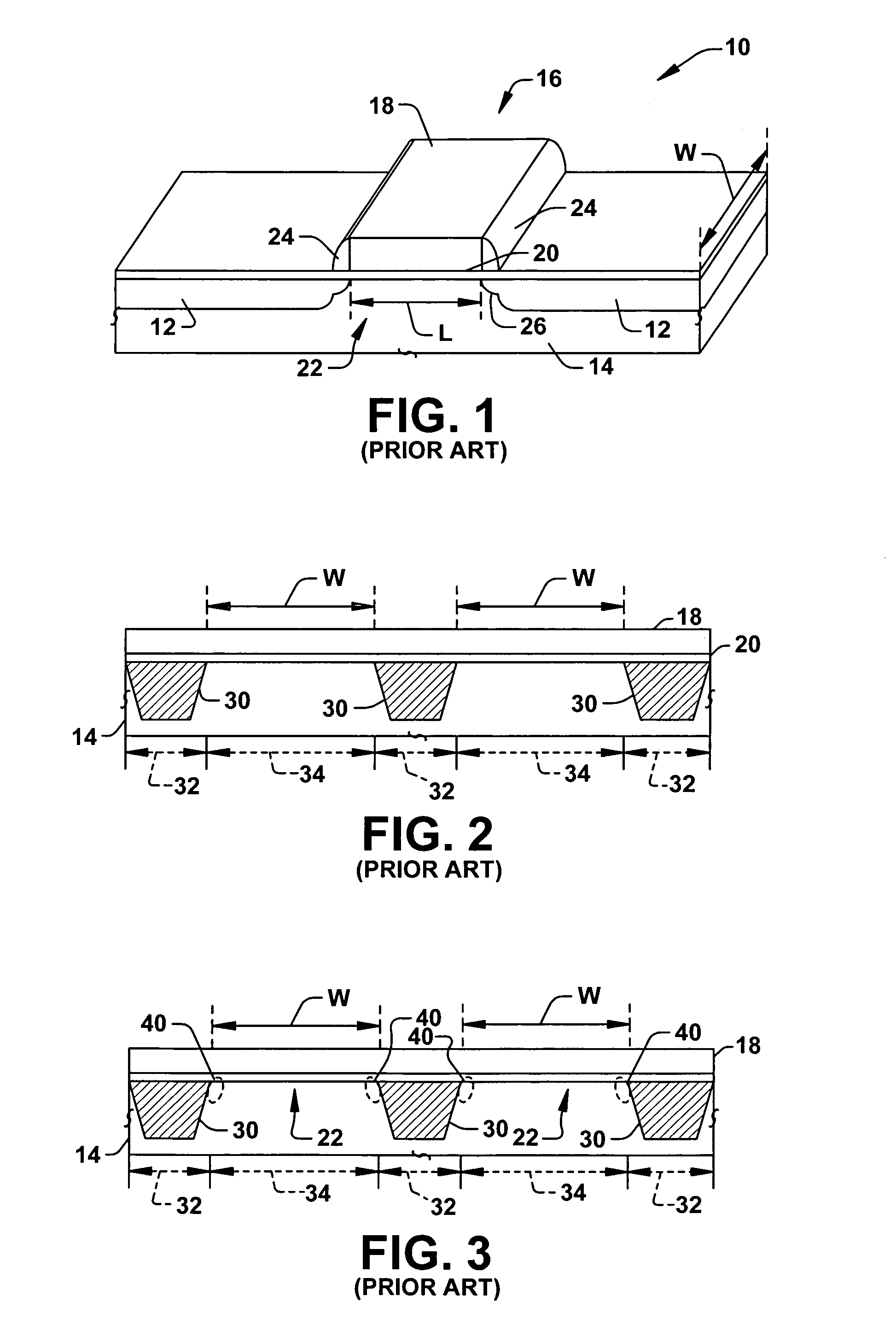
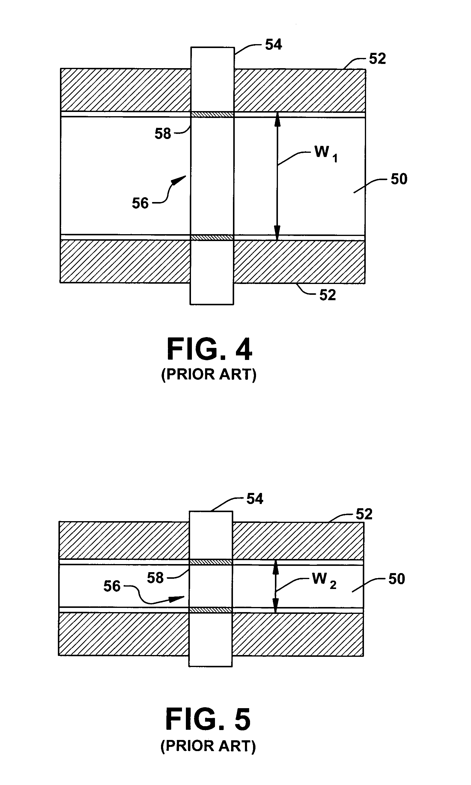
[0022]In order to fully appreciate the various aspects of the present invention, a brief description of a conventional STI fabrication process as appreciated by the inventors of the present invention will be discussed. After a discussion thereof, the various aspects of the present invention will be disclosed and more fully appreciated.
[0023]In the fabrication of semiconductor device...
PUM
 Abstract
Description
Claims
Application Information