

Pulse laser etching device used for transparent electroconductive thin film and control method of pulse laser etching device
A technology of transparent conductive film and pulsed laser, which is applied to laser welding equipment, conductors, circuits, etc., can solve the problems of increased production cost of finished products, environmental pollution, complex process, etc., and achieves reduced labor costs, high efficiency, and simple equipment operation Effect
- Summary
- Abstract
- Description
- Claims
- Application Information
AI Technical Summary
Problems solved by technology
Method used
Image

Examples
Embodiment Construction
[0018] The present invention will be further described below in conjunction with the accompanying drawings and embodiments.
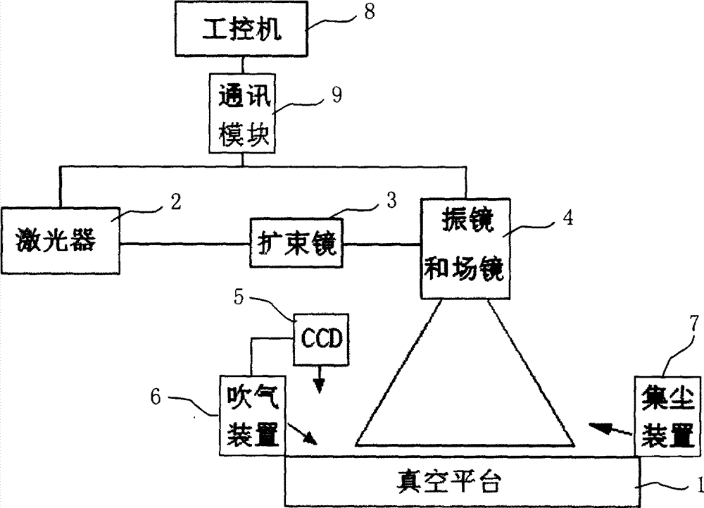
[0019] figure 1 It is a schematic structural diagram of a pulsed laser etching device for transparent conductive thin films according to the present invention.
[0020] See figure 1 The pulse laser etching device for transparent conductive thin films provided by the present invention includes a vacuum platform 1 for absorbing film materials, a laser 2 and a vibrating mirror 4, and a beam expander 3 is arranged between the laser 2 and the vibrating mirror 4 , the top of the vacuum platform 1 is provided with a CCD image sensor 5 (Charge-coupled Device, Chinese full name: charge coupled device), one side of the vacuum platform 1 is provided with an air blowing device 6, and the other side is provided with a dust collector. device7.
[0021] In the pulse laser etching device used for transparent conductive thin films provided by the present invention, t...
PUM
| Property | Measurement | Unit |
|---|---|---|
| Wavelength range | aaaaa | aaaaa |
| Pulse width | aaaaa | aaaaa |
| Frequency | aaaaa | aaaaa |
Abstract
Description
Claims
Application Information