Atomic layer deposition tantalum nitride layer to improve adhesion between a copper structure and overlying materials

Active Publication Date: 2007-04-10
TAIWAN SEMICON MFG CO LTD
View PDF10 Cites 18 Cited by
  • Summary
  • Abstract
  • Description
  • Claims
  • Application Information

AI Technical Summary

Benefits of technology

[0006]It is an object of this invention to form a capping layer on an underlying copper struc

Problems solved by technology

For example the adhesion between a copper damascene structure and overlying layers or structures, such as a silicon nitride etch stop layer,

Method used


Image

  • Atomic layer deposition tantalum nitride layer to improve adhesion between a copper structure and overlying materials
  • Atomic layer deposition tantalum nitride layer to improve adhesion between a copper structure and overlying materials
  • Atomic layer deposition tantalum nitride layer to improve adhesion between a copper structure and overlying materials

Examples


Embodiment Construction

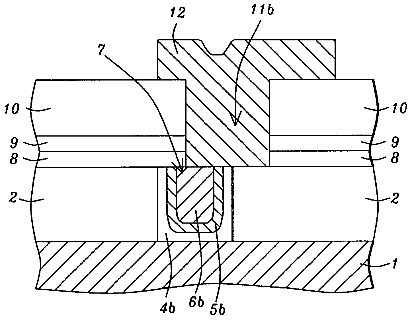
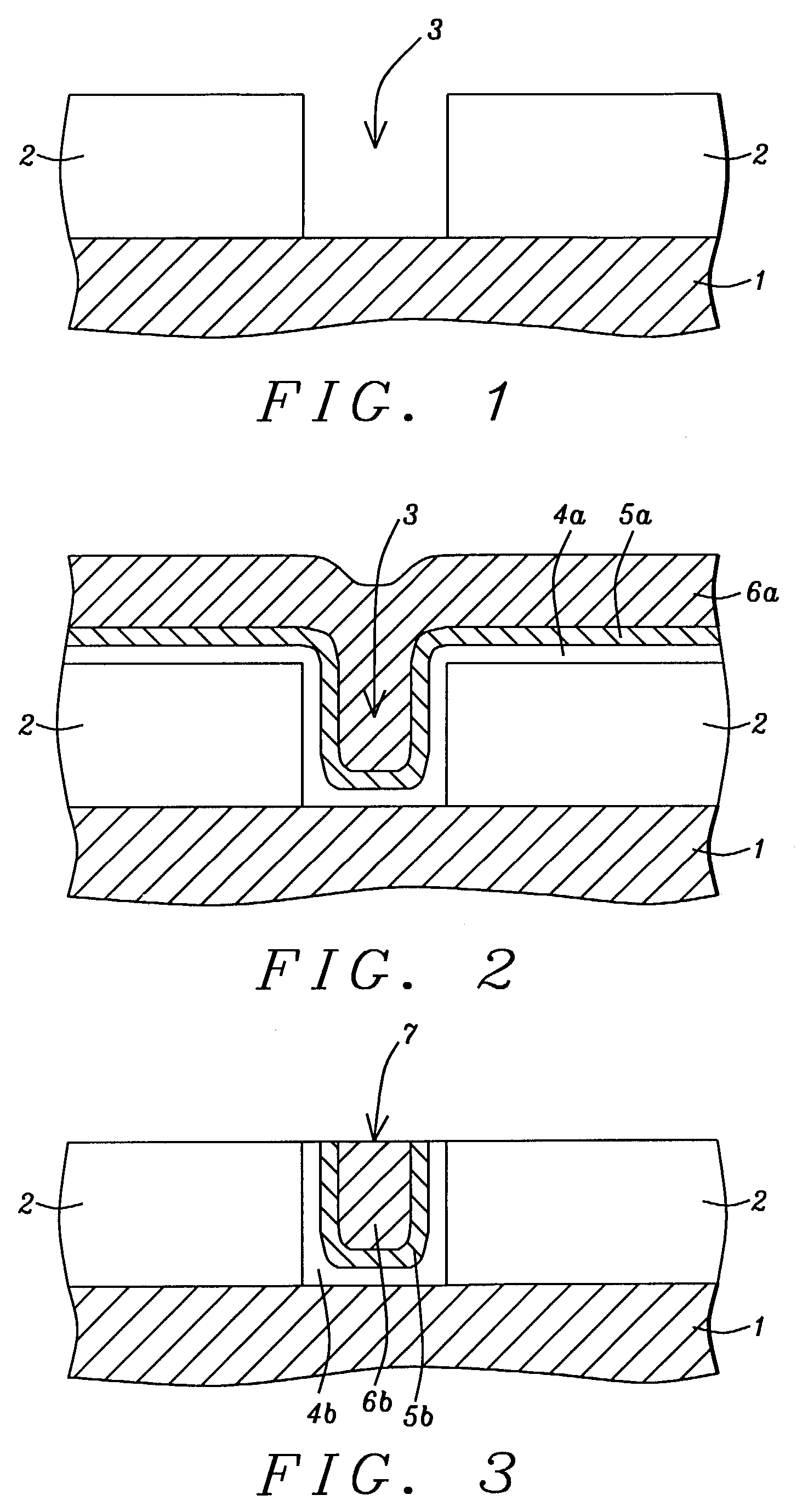
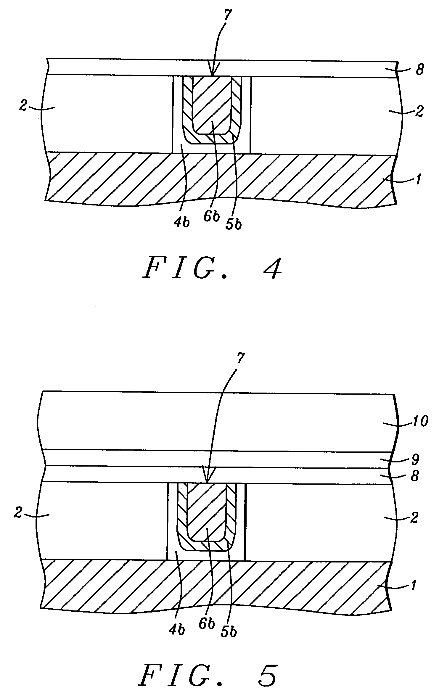
[0012]The method of forming a copper damascene structure featuring an overlying TaN capping layer, formed via ALD procedures and used to improve the adhesion between the copper damascene structure and overlying layers such as etch stop and interlevel dielectric layers, will now be described in detail. Conductive region 1, shown schematically in FIG. 1, can be an underlying, lower level metal interconnect structure, or a underlying metal via structure, comprised of either aluminum based material, copper, or tungsten. Inter-metal dielectric (IMD), layer 2, comprised of an insulator layer such as silicon oxide, or comprised of a low dielectric (low k), layer such as a fluorinated silica glass (FSG), with a dielectric constant between 3.5 to 3.8, is formed on conductive region 1, at a thickness between about 2000 to 4000 Angstroms, via chemical vapor deposition (CVD), procedures. A photoresist shape, not shown in the drawings, is formed on IMD layer 2, and used as an etch mask to allow ...


PUM


Abstract

A process for improving the adhesion between an underlying copper structure, and overlying materials and structures, has been developed. The process features formation of a tantalum nitride layer on a copper structure, wherein the copper structure is located in a damascene type opening. To obtain the maximum adhesion benefit the tantalum nitride layer is formed via an atomic deposition layer procedure, performed at specific deposition conditions. The adhesion between the underlying copper structure and overlying materials such as a silicon nitride etch stop layer, as well the adhesion between the lower level copper structure and overlying upper level metal interconnect structures, is improved as a result of the presence of the atomic layer deposited tantalum nitride layer.

Description

BACKGROUND OF THE INVENTION[0001](1) Field of the Invention[0002]The present invention relates to processes used to fabricate semiconductor devices, and more specifically to a method of forming a capping layer on a copper structure, wherein the capping layer improves the adhesion between the copper structure and overlying materials.[0003](2) Description of Prior Art[0004]Micro-miniaturization, or the ability to fabricate semiconductor devices with sub-micron features, has allowed the performance of the sub-micron devices to be increased. The use of smaller device features have resulted in a reduction of performance degrading parasitic junction capacitances enabling the desired device performance increase to be realized. In addition the use of low dielectric constant materials, as well as the use of more conductive interconnect materials such as copper, have also contributed to device performance enhancements. However the use of the above materials such as copper for interconnect str...

Claims


Application Information

Patent Timeline
IPC IPC(8): H01L21/4763H01L21/285H01L21/3205H01L21/60H01L21/768H01L23/48H01L23/52
CPCH01L21/28562H01L21/76849
Inventor LIN, JING-CHENGPENG, CHAO-HSIENSHUE, SHAU LINLIANG, MONG SONG
Owner TAIWAN SEMICON MFG CO LTD
Why Eureka
Try Eureka