Stress engineering using dual pad nitride with selective SOI device architecture

a stress engineering and selective soi technology, applied in the field of stress engineering using dual pad nitride with selective soi device architecture, can solve the problems of parasitic resistance and capacitance becoming a fundamental limiting factor, affecting electron mobility, and no longer producing the desired improvements in device performan

Active Publication Date: 2007-04-10
GLOBALFOUNDRIES U S INC
View PDF87 Cites 27 Cited by
  • Summary
  • Abstract
  • Description
  • Claims
  • Application Information

AI Technical Summary

Benefits of technology

[0007]In accordance with the present invention, high values of stress can be introduced into the channel regions of MOS devices utilizing the method of the present invention in which dual stress nitride films are employed as a pad nitride film in the MOS isolation process (e.g., STI process) in conjunction with a selective SOI device architecture. Dual stress nitride liner means that both tensile and compressive nitride films are deposited on the wafer covering the desired device regions (i.e., nFET region or pFET region). The use of the highly stressed nitride films as the pad nitride film of the isolation process does not incorporate much strain in a conventional bulk silicon wafer, which is why the selective SOI architecture is important.

Problems solved by technology

Conventional gate length and gate dielectric scaling of complementary metal oxide semiconductor (CMOS) technology no longer produces the desired improvements in device performance.
Parasitic resistances and capacitances are becoming a fundamental limiting factor to improving device performance with each new technology node.
For example, the application of compressive stress in the longitudinal direction of current flow is beneficial for hole mobility, but detrimental for electron mobility.
The application of tensile stress in the longitudinal direction is beneficial for electrons, but detrimental for holes.
Unfortunately, the use of stress liners appears to be approaching limitations in the magnitude of stress that can be applied to the channel of CMOS devices.

Method used


Image

  • Stress engineering using dual pad nitride with selective SOI device architecture
  • Stress engineering using dual pad nitride with selective SOI device architecture
  • Stress engineering using dual pad nitride with selective SOI device architecture

Examples


Embodiment Construction

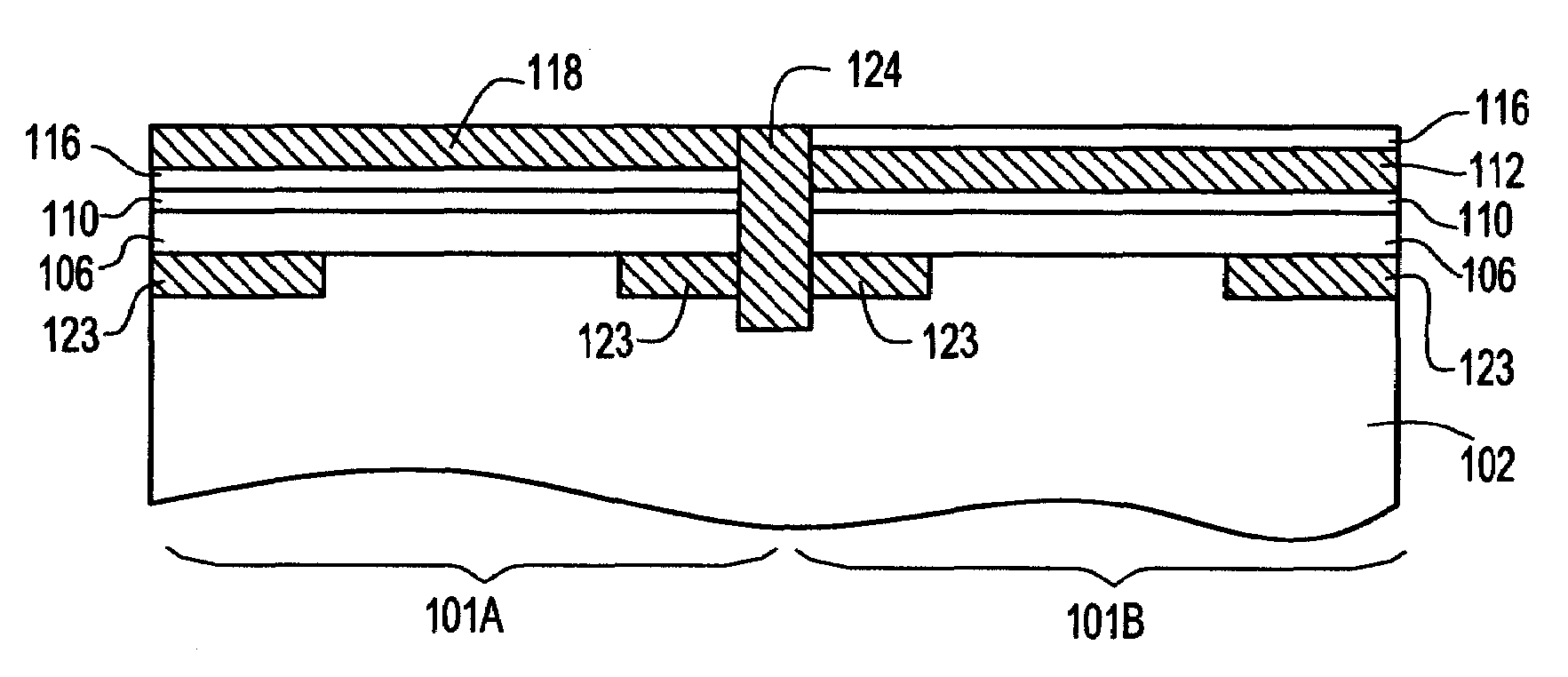
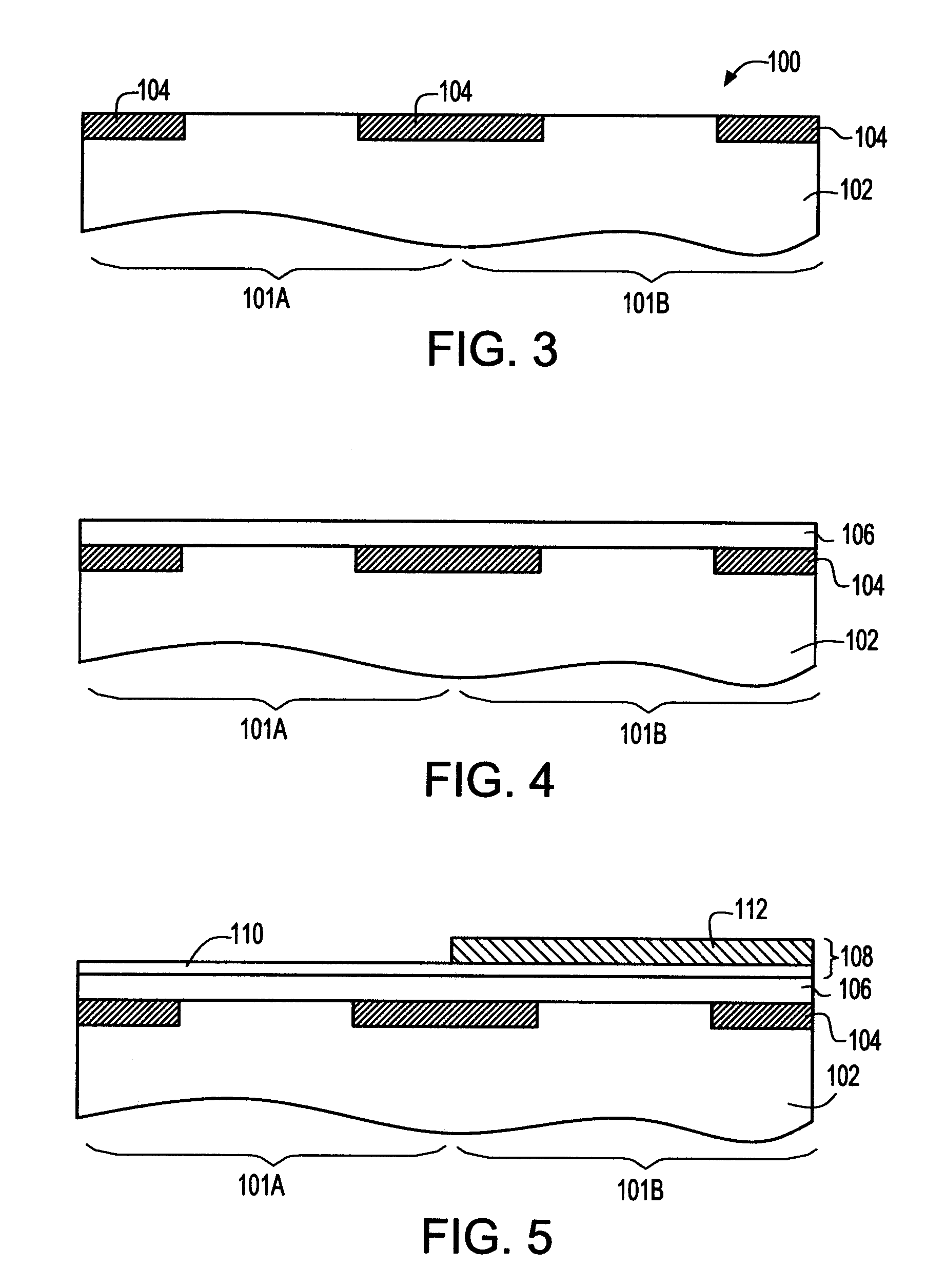
[0018]The present invention, which provides a method for engineering stress in the channel regions of MOS transistors of different conductivities as well as the structure formed utilizing the same, will now be described in greater detail by referring to the following description and drawings that accompany the present application. It is noted that the drawings of the present application are provided for illustrative purposes and, as such, they are not drawn to scale.

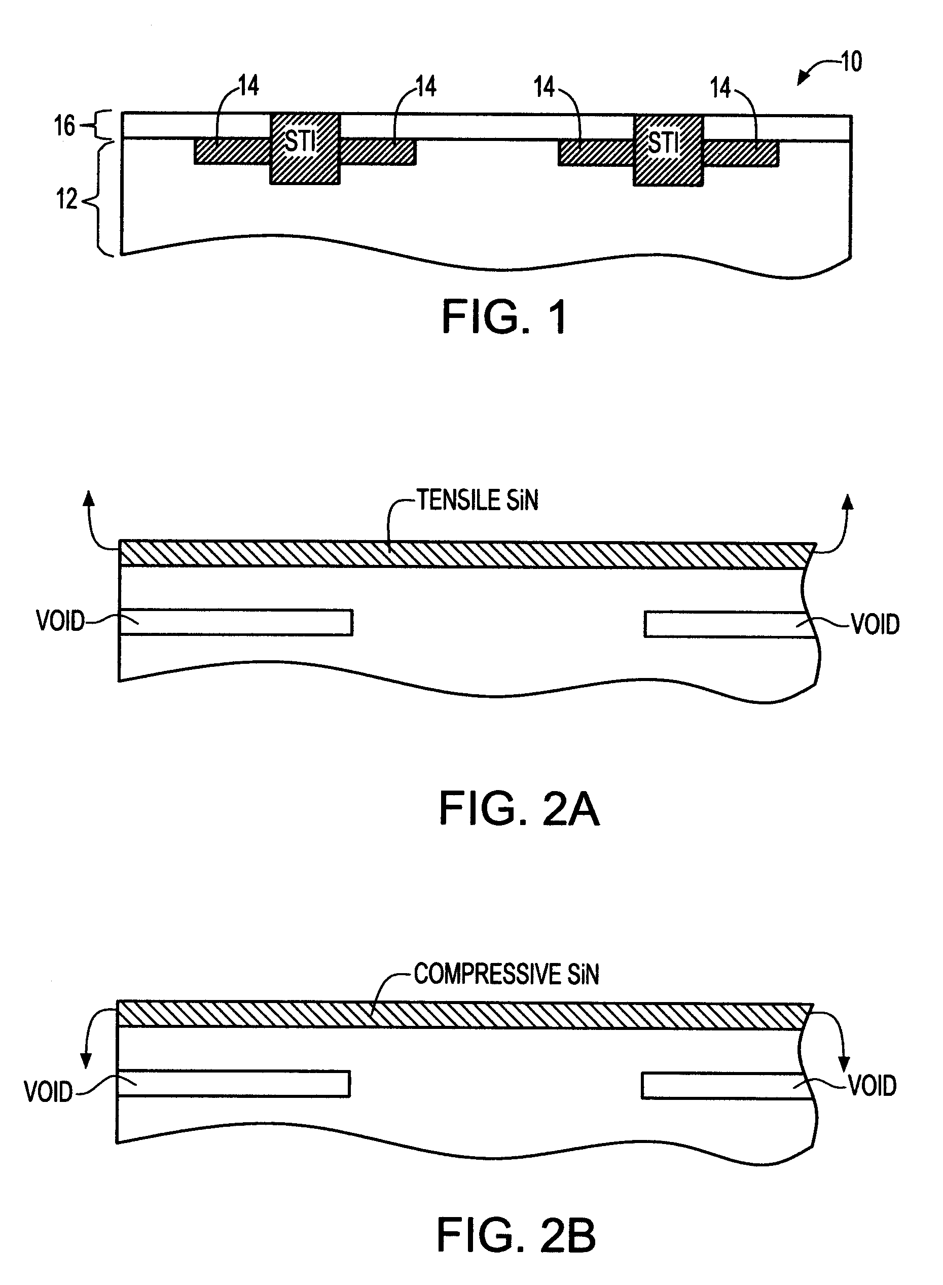
[0019]In accordance with the present invention, there are two key features that enable a large amount of stress to be applied to the channel of MOS devices: (1) the use of dual stress nitride films as the pad nitride in the STI isolation process and, (2) the dual nitride isolation process must be applied to a structure that will subsequently have a selective SOI device architecture. Dual stress nitride liner means that both tensile and compressive nitride films are deposited on the wafer covering the desired device regio...


PUM

PropertyMeasurementUnit
thicknessaaaaaaaaaa
thicknessaaaaaaaaaa
thicknessaaaaaaaaaa

Abstract

A method for engineering stress in the channels of MOS transistors of different conductivity using highly stressed nitride films in combination with selective semiconductor-on-insulator (SOI) device architecture is described. A method of using compressive and tensile nitride films in the shallow trench isolation (STI) process is described. High values of stress are achieved when the method is applied to a selective SOI architecture.

Description

FIELD OF THE INVENTION[0001]The present invention relates to semiconductor device manufacturing, and more particularly to a method for engineering stress in channel regions of metal-oxide-semiconductor (MOS) devices of different conductivities using highly stressed nitride films in combination with a selective semiconductor-on-insulator (SOI) device architecture. Specifically, the inventive method uses compressive and tensile nitride films as the dual pad nitride in a shallow trench isolation (STI) process to induce stress in the channel regions of MOS transistors. High values of stress are achieved when the inventive method is applied to a selective SOI device architecture. The present invention also relates to the semiconductor structure that is manufactured utilizing the method of the present application.BACKGROUND OF THE INVENTION[0002]Conventional gate length and gate dielectric scaling of complementary metal oxide semiconductor (CMOS) technology no longer produces the desired ...

Claims


Application Information

Patent Timeline
Patent Type & Authority Patents(United States)
IPC IPC(8): H01L31/00
CPCH01L21/823807H01L21/823814H01L21/823878H01L21/84H01L27/1203H01L29/0653H01L29/7842
Inventor CHIDAMBARRAO, DURESETIHENSON, WILLIAM K.RIM, KERNWILLE, WILLIAM C.
Owner GLOBALFOUNDRIES U S INC
Why Eureka
Try Eureka