Automated test of receiver sensitivity and receiver jitter tolerance of an integrated circuit

a technology of integrated circuits and automatic testing, applied in the direction of noise figure or signal-to-noise ratio measurement, instruments, transmission monitoring, etc., can solve the problems of significant lower performance of automated testing equipment, historical difficulty in testing integrated circuits intended to communicate signals at extremely high frequencies, and different noise environmen

Active Publication Date: 2007-04-10
TEXAS INSTR INC
View PDF10 Cites 33 Cited by
  • Summary
  • Abstract
  • Description
  • Claims
  • Application Information

AI Technical Summary

Benefits of technology

[0023]It is a further object of this invention to provide such an apparatus and method that may be implemented in a low-cost yet programmable manner in automated test equipment.
[0024]It is a further object of this invention to provide such an apparatus and method in which the desired jitter and attenuation can be precisely set and remain repeatable at high frequencies.

Problems solved by technology

The testing of integrated circuits that are intended to communicate signals at extremely high frequencies is an historically difficult problem.
Typically, automated test equipment is constructed from circuitry that has significantly lower performance than the state-of-the-art circuits that are to be tested by that equipment.
In addition, the test socket and other peripheral connectors and circuitry that interface with each device being tested typically present a different noise environment (often a noisier environment) than the device may face in its end use.
Accordingly, the test results of modern automated test equipment may be in error, causing both false failed devices (i.e., devices that in fact meet the specifications but fail the test), and also false passed devices (i.e., devices that do not in fact meet the specifications but pass the test).
Complicating this problem is the extremely high cost of integrated circuit testing.
The cost of test equipment having even moderate performance characteristics is extremely high, with modern testers often costing as much as $1 million or more each.
Today's modern integrated circuit devices are also very complex, with many devices having hundreds of thousands of transistors and logic gates, each of which require some sort of electrical test to ensure complete functionality.
This complexity in turn increases (in some cases, geometrically) the time required to functionally test a device, which of course also increases the test cost.
In short, the testing trends for modern integrated circuits generally involves increasingly expensive testers for increasingly longer test times per device.
A particularly difficult test problem is the testing of high-frequency data receiver circuits in modern integrated circuits.
For the reasons mentioned above, this test requirement can be quite costly.
From a test standpoint, however, this conventional setup obviously does not test for the parameters of receiver sensitivity and receiver jitter tolerance.
Accordingly, following conventional automated loopback techniques, 100% manufacturing testing of these parameters is not practicable.
While one could theoretically program the output levels from the transmitter to be produced at lower voltage swings, and while one could vary the timing of the differential crossover points to simulate jitter, this type of iterative testing would significantly add to device test times, and thus significantly increase test costs.

Method used


Image

  • Automated test of receiver sensitivity and receiver jitter tolerance of an integrated circuit
  • Automated test of receiver sensitivity and receiver jitter tolerance of an integrated circuit
  • Automated test of receiver sensitivity and receiver jitter tolerance of an integrated circuit

Examples


Embodiment Construction

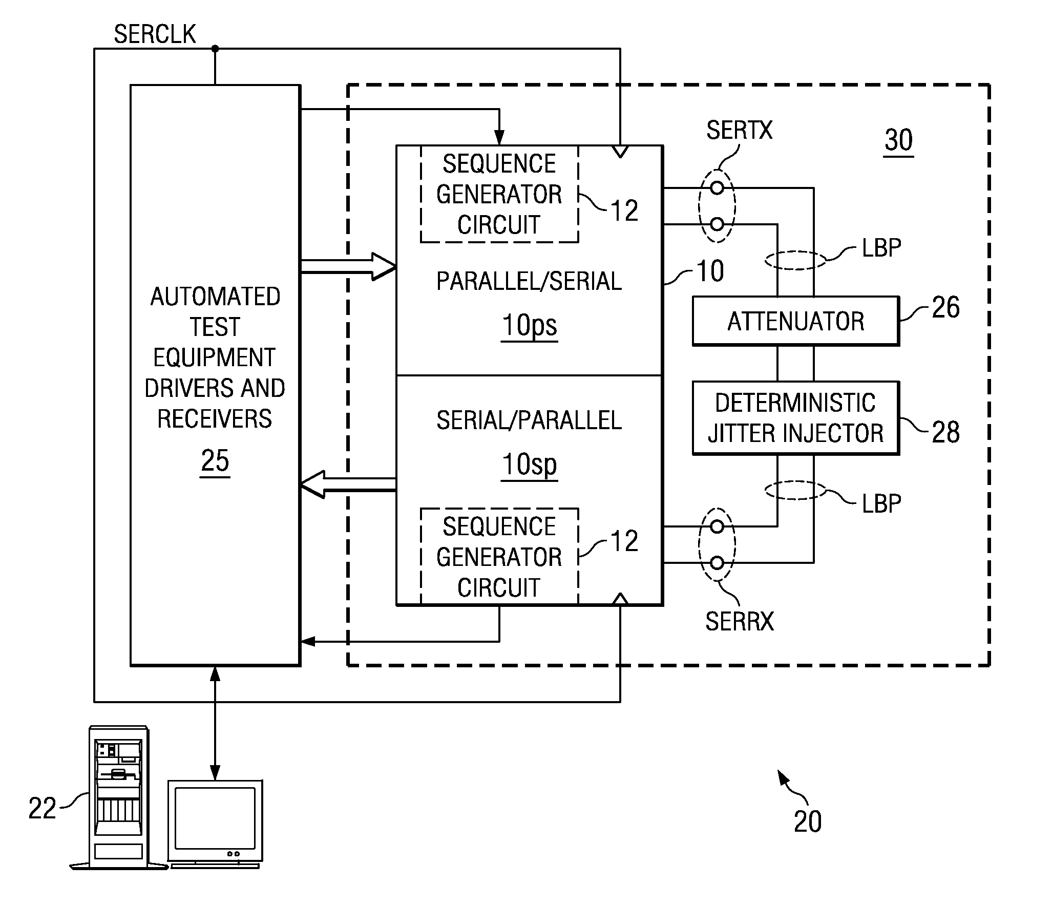
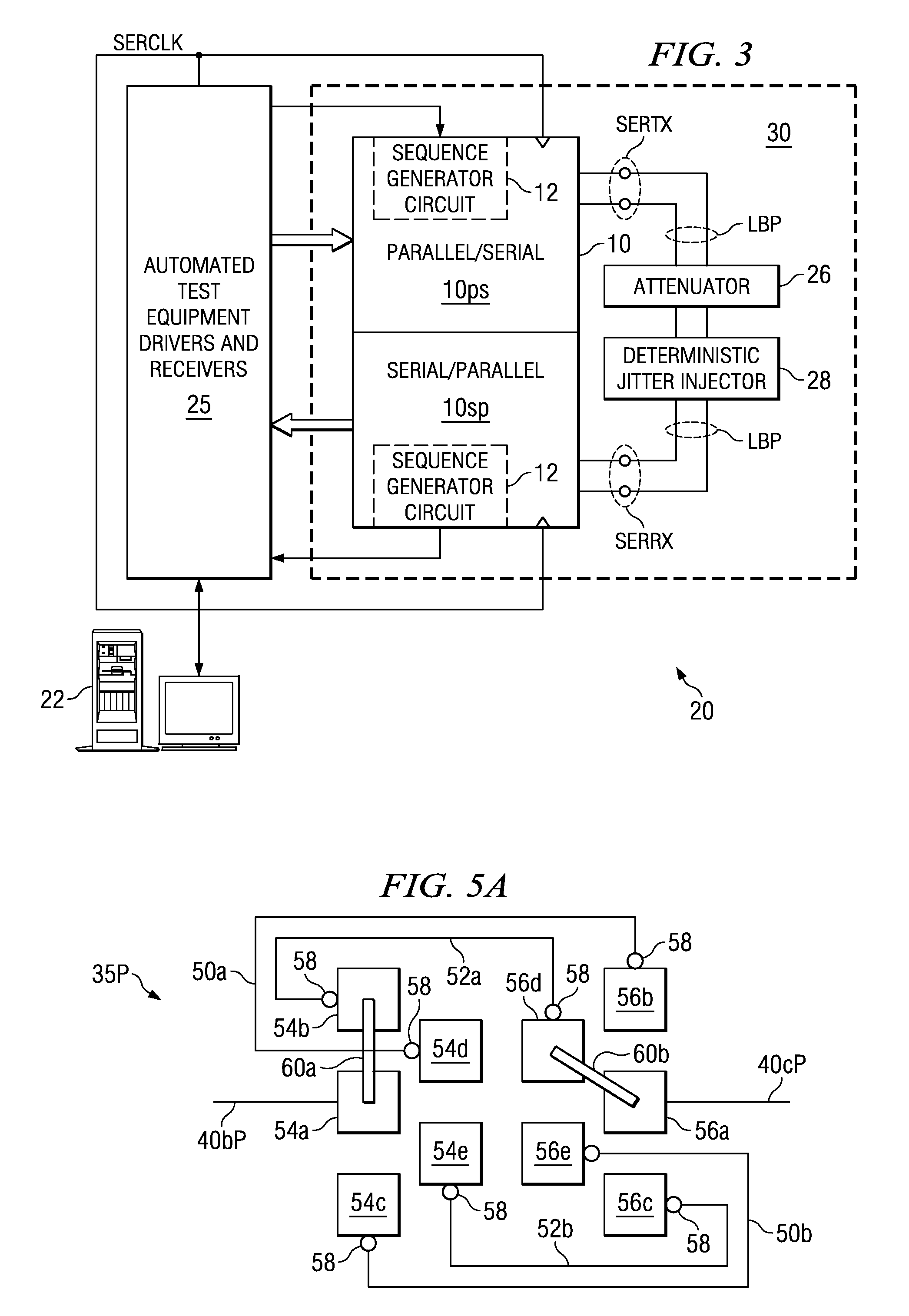
[0033]The present invention will be described in connection with its preferred embodiment, namely as implemented into automated test equipment for high-speed communications integrated circuits, such as a serializer / deserializer transceiver device, considering that this invention is especially beneficial when implemented into such an environment. However, it is contemplated that this invention may also provide benefits when used in the automated testing of other types of integrated circuit devices, and also in the automated testing of other electronic components. Accordingly, it is to be understood that the following description is provided by way of example only, and is not intended to limit the true scope of this invention as claimed.

[0034]Referring now to FIG. 3, the electrical construction of an automated test apparatus 20, for testing SerDes device 10 according to the preferred embodiment of the invention, will now be described. Automated test apparatus 20 includes ATE drivers a...


PUM


Abstract

An automated test system (20) for testing a high-speed communications integrated circuit (10), such as a serializer / deserializer, is disclosed. The system (20) is able to test the parameters of receiver jitter tolerance and receiver sensitivity in a loopback connection arrangement, in which serial output terminals (SERTX) of the integrated circuit (10) are connected to serial input terminals (SERRX) of the integrated circuit (10). An attenuator (26), which in the disclosed embodiment includes programmable attenuators (30P, 30N) and a fixed attenuator (32), one of which is selected, is disposed in the loopback path. A deterministic jitter injector (28) is also in the loopback path, and may be implemented by way of variable length trace blocks (35P, 35N) on the test board (30). In this way, the serial output signals generated by the integrated circuit (10) are modified by the attenuator (26) and deterministic jitter injector (28) so that the signal as received at the serial input terminals (SERRX) can be at the specification limits of the circuit (10).

Description

CROSS-REFERENCE TO RELATED APPLICATIONS[0001]Not applicable.STATEMENT REGARDING FEDERALLY SPONSORED RESEARCH OR DEVELOPMENT[0002]Not applicable.BACKGROUND OF THE INVENTION[0003]This invention is in the field of integrated circuit testing, and is more specifically directed to the testing of high speed data receiver and transceiver circuits.[0004]Each modern integrated circuit device is typically subjected to electrical testing at least once during the process of its manufacture. In many cases, integrated circuits are functionally tested when in wafer form, to avoid the cost of packaging an integrated circuit device that is not functional or otherwise cannot meet its specified requirements. Packaged integrated circuits are also typically functionally tested in the manufacturing flow, to ensure that the devices not only function but actually meet the speed and power requirements desired by the customer and guaranteed by the manufacturer. Conventional manufacturing testing is often refe...

Claims


Application Information

Patent Timeline
Patent Type & Authority Patents(United States)
IPC IPC(8): H04B17/00G01R31/317H04Q7/20
CPCG01R31/31709G01R31/31716
Inventor BOOSE, WILLIAM CLAYDAVIS, VERNON D.HANISH, PETER D.
Owner TEXAS INSTR INC
Why Eureka
Try Eureka