In-situ pre-coating of plasma etch chamber for improved productivity and chamber condition control

a technology of plasma etching and in-situ pre-coating, which is applied in the direction of vacuum evaporation coating, coating, chemistry apparatus and processes, etc., can solve the problems of affecting the uniformity and accuracy of critical dimensions, and affecting the quality of plasma etching

Inactive Publication Date: 2007-04-17
LAM RES CORP
View PDF18 Cites 95 Cited by
  • Summary
  • Abstract
  • Description
  • Claims
  • Application Information

AI Technical Summary

Benefits of technology

[0011]Broadly speaking, the present invention fills these needs by providing a method and apparatus for in-situ cleaning of a process chamber that provides a removable coating to the inner surfaces of the process chamber. The removable coating, known as pre-coat, allows for consistent starting conditions for each wafer being processed. It should be appreciated that the present invention may be implemented in numerous ways, including as an apparatus, a system, a device, or a method. Several inventive embodiments of the present invention are described below.

Problems solved by technology

As semiconductor processes deal with smaller geometries being defined on semiconductor substrates it is becoming more difficult to maintain the uniformity and accuracy of critical dimensions.
As these deposits accumulate over time, they can become a source of particulate contamination that is harmful to the substrates being processed.
For example, the particulate contamination may flake off and fall onto the surface of the substrate if the particulate contamination is allowed to build up over time.
Although care and caution is involved during the monitoring of a chemical process, more often than not, undesired residues are deposited on the inner surfaces of the process chambers where the processes are taking place.
The undesired residues, unfortunately, get deposited in and around the walls of the processing chamber.
The build up of residues inside the processing chamber, over time, not only make the processes unreliable and shifted from baseline, but also result in degraded, defective substrates due to particulate contamination that builds up over time on the inner surfaces of the chamber.
In addition, process etch rates or deposition rates can vary over time due to the changing chamber conditions from residue build-up resulting in out of control process performance.
As alluded to above, the build up of deposits on the inner surfaces of the chamber causes an inconsistent environment which impacts the processing operation being performed.
Accordingly, the changed starting conditions for each successive processing operation causes a variance that eventually exceeds acceptable limits, which results in etch rate drift, critical dimension drift, profile drift, etc.
However, these cleaning processes tend to leave residues of their own behind.
Thus, as a result of attempting to clean the processing chamber of one contaminant, the cleaning process leaves behind another residue that may build up over time and eventually flake off onto a semiconductor substrate.
In addition, failure to completely clean the etch chamber affects the processing of the next semiconductor substrate.
Thus, the system availability is adversely impacted because of the restricted mean time between wet cleans.
As more residue 110 accumulates on the inner surfaces, the impact on the processing operation, such as an etch operation, becomes more severe because of the residue buildup.
Unfortunately, such cleaning operations affect a substrate processing system's utilization in a variety of ways.
When a wet clean is performed, opening the processing chamber and physically wiping the chamber's interior surfaces results in even more downtime because the processing environment must subsequently be re-stabilized.

Method used


Image

  • In-situ pre-coating of plasma etch chamber for improved productivity and chamber condition control
  • In-situ pre-coating of plasma etch chamber for improved productivity and chamber condition control
  • In-situ pre-coating of plasma etch chamber for improved productivity and chamber condition control

Examples


Embodiment Construction

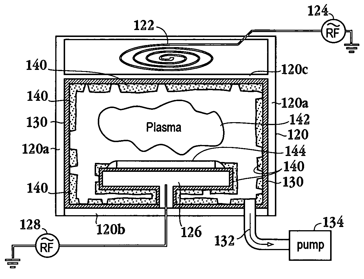
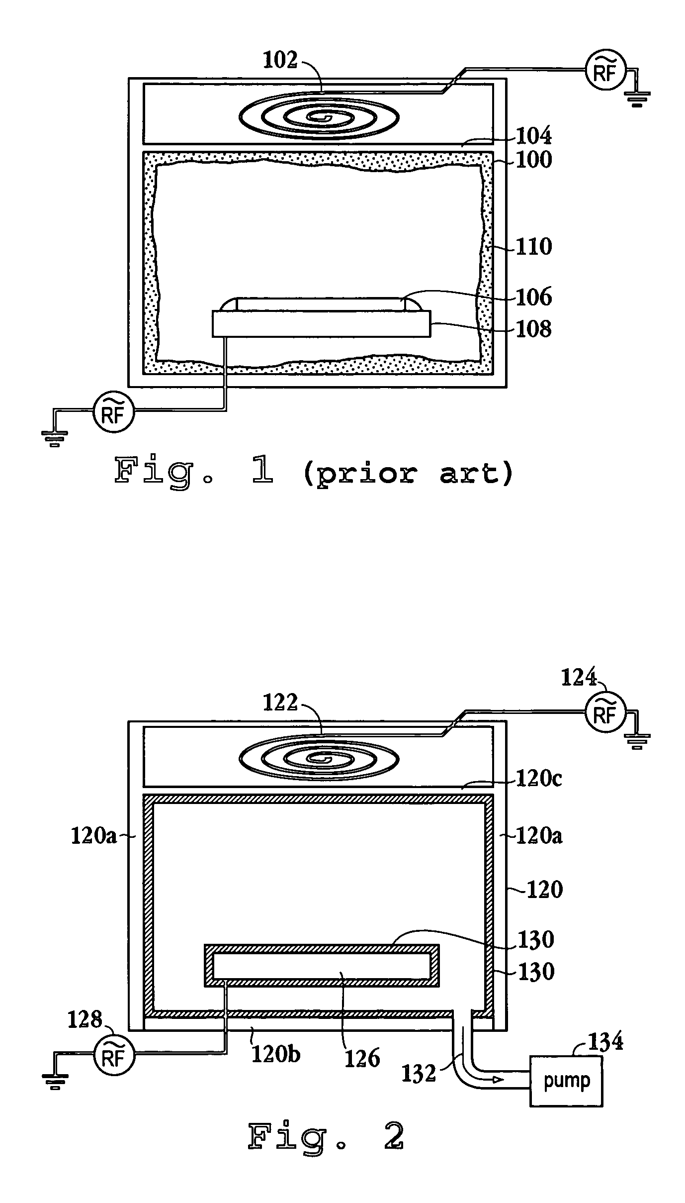
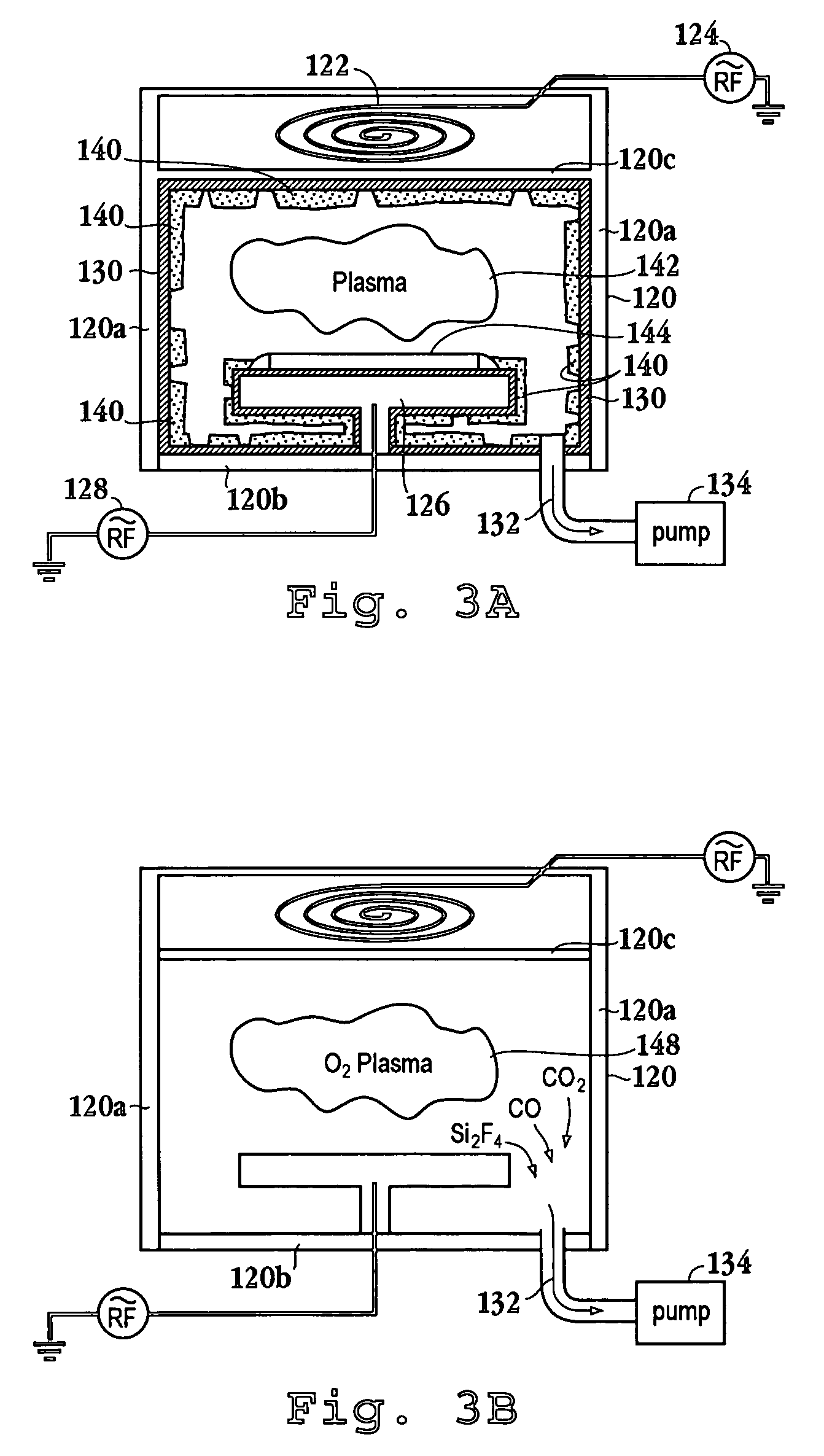
[0031]An invention is described which provides a method and apparatus for providing the same starting conditions for the plasma processing of each wafer in a series of wafers. The same starting conditions are provided by applying a carbon-containing polymer coating or silicon-containing coating to the inner surfaces of the plasma processing chamber prior to introduction of the wafer. The pre-coat layer applied on the inner surfaces of the chamber also prevents the transfer of particulate and metal contamination from chamber surfaces to the subsequent wafer processed in the semiconductor reactor. It will be obvious, however, to one skilled in the art, that the present invention may be practiced without some or all of these specific details. In other instances, well known process operations have not been described in detail in order not to obscure the present invention.

[0032]The embodiments of the present invention provide a method and apparatus for applying a carbon and fluorine (CFx...


PUM

PropertyMeasurementUnit
thicknessaaaaaaaaaa
thicknessaaaaaaaaaa
energyaaaaaaaaaa

Abstract

A semiconductor processing chamber having a silicon containing pre-coat is provided. The chamber includes a top electrode in communication with a power supply and a processing chamber defined within a base, a sidewall extending from the base, and a top disposed on the sidewall. The processing chamber has an outlet enabling removal of fluids within the processing chamber and includes a substrate support where an outer surface of the substrate support coated with the removable silicon containing coating, wherein the silicon containing coating is a compound consisting essentially of silicon and one of bromine and chlorine. The chamber includes an inner surface defined by the base, the sidewall and the top, where the inner surface is coated with a removable silicon containing coating.

Description

CROSS REFERENCE TO RELATED APPLICATIONS[0001]This application is a continuation-in-part of application Ser. No. 10 / 186,917, filed on Jun. 28, 2002 now U.S. Pat. No. 6,776,851. The disclosure of this application is incorporated herein by reference for all purposes.BACKGROUND OF THE INVENTION[0002]1. Field of the Invention[0003]This invention generally relates to an apparatus and method of cleaning a processing chamber to remove previously deposited chamber residues, which have accumulated on interior surfaces of the apparatus. In particular, the invention relates to a silicon-containing coating being applied to the inner surfaces of a processing chamber where the silicon-containing coating is removed along with any residues deposited on the coating during processing operations.[0004]2. Description of the Related Art[0005]As semiconductor processes deal with smaller geometries being defined on semiconductor substrates it is becoming more difficult to maintain the uniformity and accura...

Claims


Application Information

Patent Timeline
Patent Type & Authority Patents(United States)
IPC IPC(8): C23F1/00C23C16/44
CPCC23C16/4404C23C16/4405H01J37/321H01J37/32862Y10S134/902Y10S438/905
Inventor SINGH, HARMEETULLAL, SAURABH J.GANGADHARAN, SHIBU
Owner LAM RES CORP
Why Eureka
Try Eureka