Micro-feature fill process and apparatus using hexachlorodisilane or other chlorine-containing silicon precursor

a technology of silicon precursor and micro-feature, which is applied in the field of semiconductor processing, can solve problems such as forming voids, and achieve the effect of cost-effectiveness

Active Publication Date: 2007-04-17
TOKYO ELECTRON LTD
View PDF8 Cites 54 Cited by
  • Summary
  • Abstract
  • Description
  • Claims
  • Application Information

AI Technical Summary

Benefits of technology

[0007]In order to prevent void formation caused by higher relative deposition rates occurring at the top of a micro-feature, conventional micro-feature filling techniques reduce overall deposition rates during the initial stages of deposition. The deposition rate is reduced when SiH4 is combined with an inert gas, or the process temperature is reduced. Neither method reduces void formation to zero, especially when the micro-features have high aspect ratios.
[0012]An object of the present invention is to provide a method and system for filling a micro-feature on a semiconductor wafer in a process chamber of a processing system which reduces or solves the above described and / or other problems with conventional deposition systems and methods.
[0013]Still another object of the present invention is to provide a cost effective mechanism for integrating silicon-containing films with semiconductor applications.

Problems solved by technology

Therefore, the higher the aspect ratio of the micro-feature the more likely the micro-feature opening will close prematurely, thus forming a void.

Method used


Image

  • Micro-feature fill process and apparatus using hexachlorodisilane or other chlorine-containing silicon precursor
  • Micro-feature fill process and apparatus using hexachlorodisilane or other chlorine-containing silicon precursor
  • Micro-feature fill process and apparatus using hexachlorodisilane or other chlorine-containing silicon precursor

Examples


Embodiment Construction

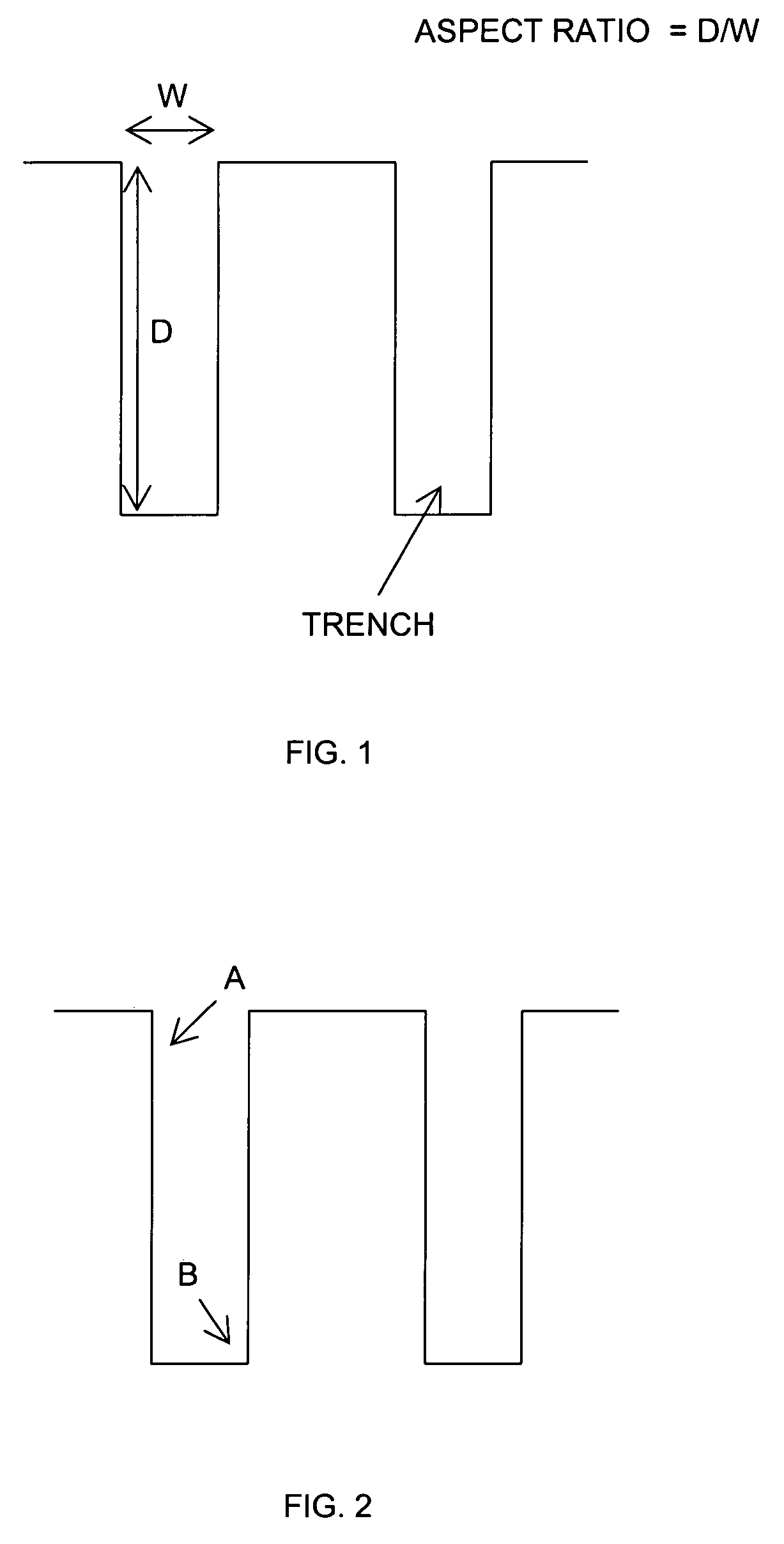
[0026]The term micro-feature, as used herein, refers to a feature formed in a substrate and / or in a layer or layers formed on a substrate that has dimensions on the micrometer scale, and typically the sub-micron scale, i.e., less than 1 μm. The micro-feature can, for example, be a trench, a hill, a valley, or a via hole.

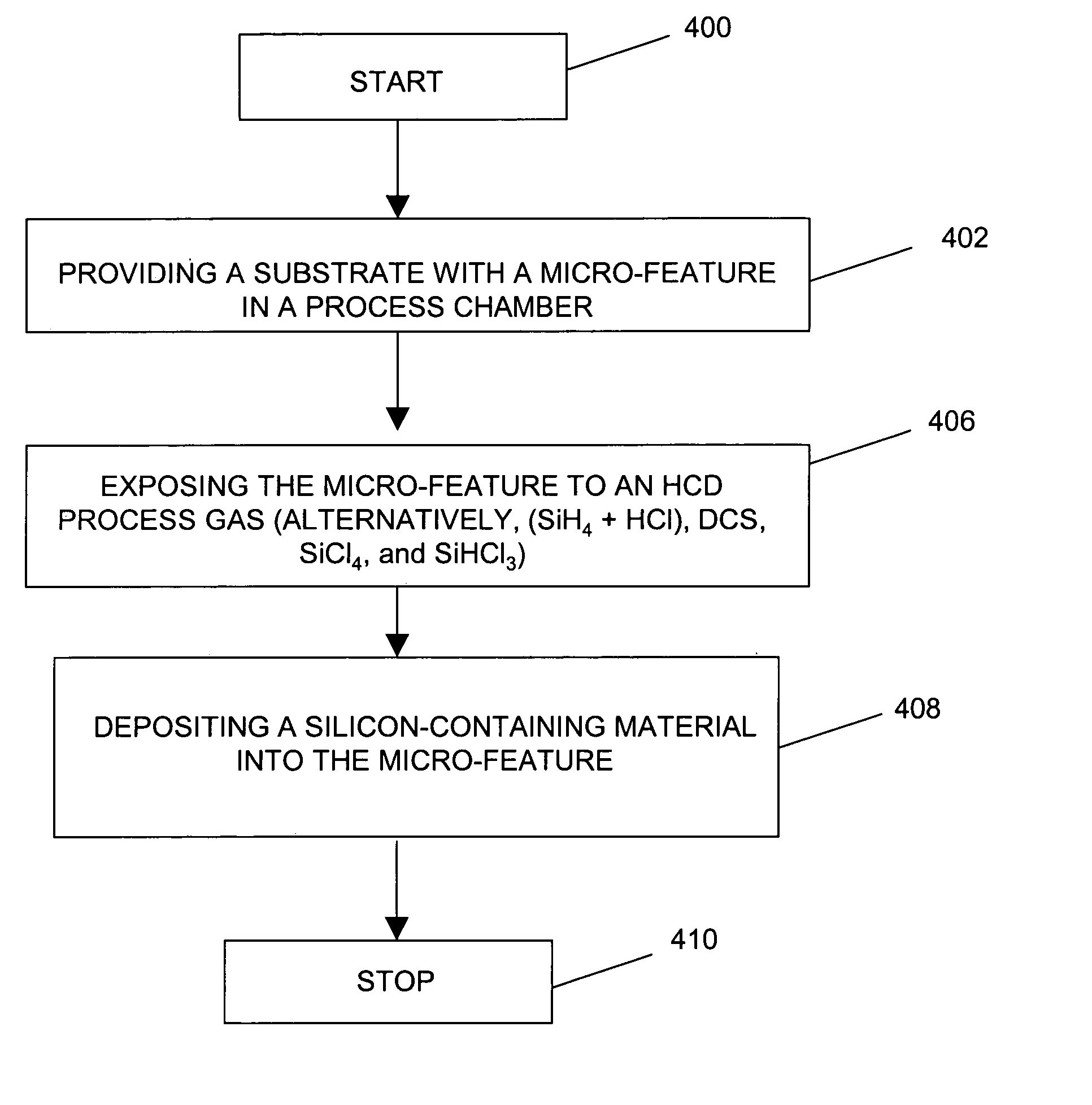
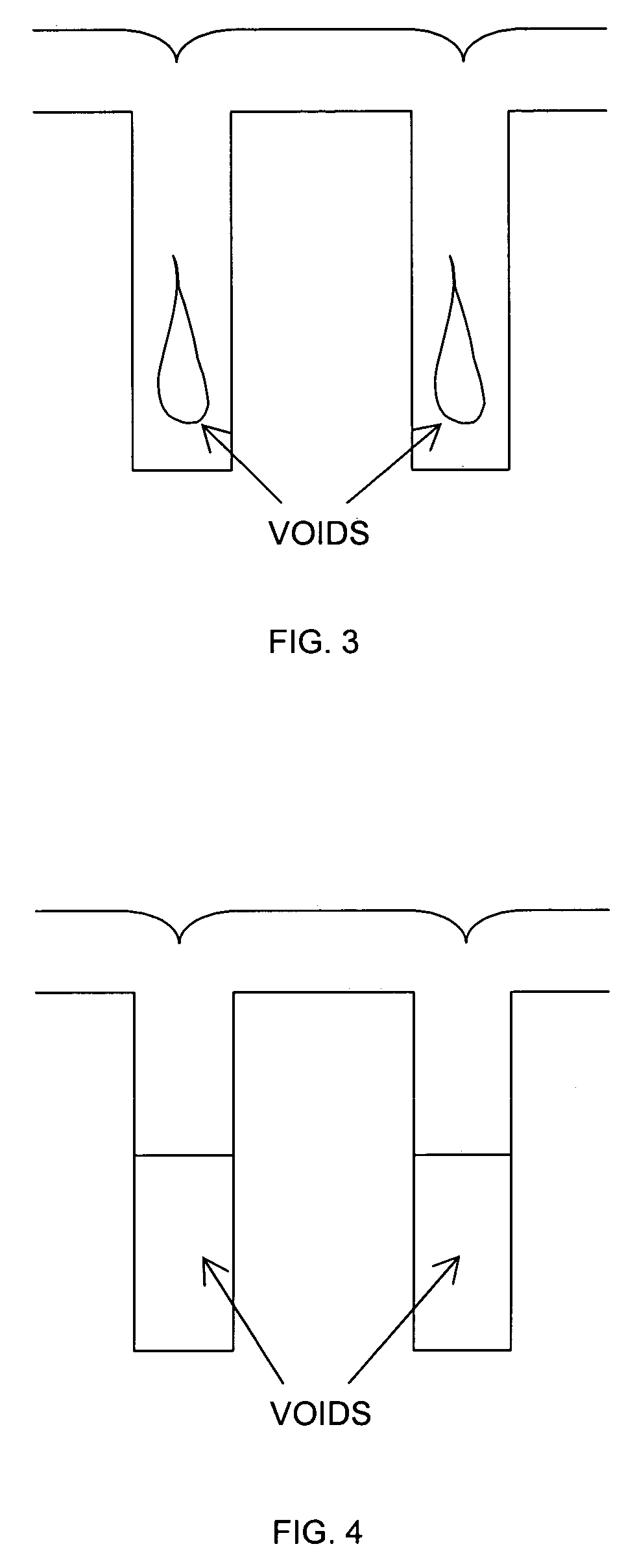
[0027]An exemplary embodiment of the invention details the use of HCD, or another chlorine-containing silicon precursor, as the main deposition gas for poly-silicon micro-feature fill. The deposition characteristics of HCD make it an ideal gas for this purpose. The deposition rate when using HCD is much lower at most operating temperatures than SiH4. HCD is also a reaction limited deposition rather than a transport limited deposition. This reduces the problem of premature closing of the opening of the micro-feature because reactants are better able to reach the bottom of the micro-feature.

[0028]Additionally, unlike SiH4, HCD contains no hydrogen. Therefore, the depos...


PUM

PropertyMeasurementUnit
pressureaaaaaaaaaa
pressureaaaaaaaaaa
pressureaaaaaaaaaa

Abstract

A method is provided for depositing a silicon-containing film in a micro-feature on a substrate by a low pressure deposition process in a processing system. A silicon-containing film can be formed in a micro-feature by providing a substrate in a process chamber of a processing system, and exposing a hexachlorodisilane (HCD) process gas to the substrate. A processing tool containing a processing system for forming a silicon-containing film in a micro-feature using a silicon and chlorine-containing gas such as a HCD process gas is provided. Alternatively, the micro-feature can be exposed to DCS, SiCl4, and SiHCl3 gases. Alternatively, the micro-feature can be exposed to (SiH4+HCl).

Description

CROSS-REFERENCE TO RELATED APPLICATIONS[0001]The present patent document is related to U.S. application Ser. No. 10 / 673,375 filed on Sep. 30, 2003, the entire contents of which are herein incorporated by reference.FIELD OF THE INVENTION[0002]The present invention relates to semiconductor processing, and more particularly, to a process and a processing tool for filling a micro-feature on a semiconductor substrate using hexachlorodisilane (HCD) process gas.BACKGROUND OF THE INVENTION[0003]During the fabrication of semiconductor devices, micro-features on the surface of the substrate are sometimes created in order to isolate devices or to create other devices such as capacitors etc. These micro-features are later filled, often by using silane (SiH4). As circuit geometries shrink to ever smaller feature sizes, the aspect ratios (ratio of depth to width) of micro-features on substrates increase, see FIG. 1. When using a silane only, poly-silicon fill process, the level of defects inside ...

Claims


Application Information

Patent Timeline
Patent Type & Authority Patents(United States)
IPC IPC(8): H01L21/336H01L21/8234
CPCC23C16/045C23C16/24H01L21/32055H01L21/76877H01L21/8234
Inventor LEITH, ALLEN JOHNDIP, ANTHONYOH, SEUNGHO
Owner TOKYO ELECTRON LTD
Why Eureka
Try Eureka