
Method of manufacturing an LCD having the amorphous portion of a transparent conductive layer removed

a technology of transparent conductive layer and manufacturing method, which is applied in the direction of semiconductor devices, semiconductor/solid-state device details, instruments, etc., can solve the problems of inability to see the display so well, disadvantageous power consumption conservation, and inconsiderable power consumption of transmission-type display devices, so as to reduce the normal uneven shape and the effect of steps used

Inactive Publication Date: 2007-05-01
SEMICON ENERGY LAB CO LTD
View PDF29 Cites 44 Cited by
  • Summary
  • Abstract
  • Description
  • Claims
  • Application Information

AI Technical Summary

Benefits of technology

[0021]By using the above-described method, photolithography steps used in forming the uneven shape normally can be reduced and therefore, considerable cost reduction and promotion of productivity can be realized.

Problems solved by technology

Power consumption of a transmission type display device is inconsiderable for driving only a display.
For use of a portable telephone, an EL back light is generally used, however, power is separately needed for the back light and a characteristic of conservation of power consumption particularly to a liquid crystal is not fully utilized, which is disadvantageous in conservation of power consumption.
Further, although in a dark environment, display of a display is viewed with excellent contrast, in an ordinary bright environment, the display is not viewed so well and there is a drawback in adaptability in accordance with the environment of use both in cases of an upper emitting type and a lower emitting type.
However, similar to the case of the transmission type liquid crystal display device, although in a dark environment, display of a display is viewed excellently, in an ordinary bright environment, the display is not viewed so well and therefore, there is still a drawback in adaptability in accordance with an environment of use both in cases of the upper emitting type and the lower emitting type.
Further, quite contrary to the former two, although in a bright environment, display of a display is viewed excellently, in a dark environment, the display is not viewed so well.
Considering the use of a portable information terminal, the portable information terminal is mainly used outdoors and there is frequently a case of viewing the display in a comparatively bright environment, however, this is still insufficient in terms of adaptability in accordance with an environment of use.
When a display is fabricated under such a state, a display having very poor optical recognizing performance is brought about.
An increase in the number of steps brings about a disadvantageous situation of a reduction in yield, extension in process time, or an increase in cost.

Method used


Image

  • Method of manufacturing an LCD having the amorphous portion of a transparent conductive layer removed
  • Method of manufacturing an LCD having the amorphous portion of a transparent conductive layer removed
  • Method of manufacturing an LCD having the amorphous portion of a transparent conductive layer removed

Examples


example 1

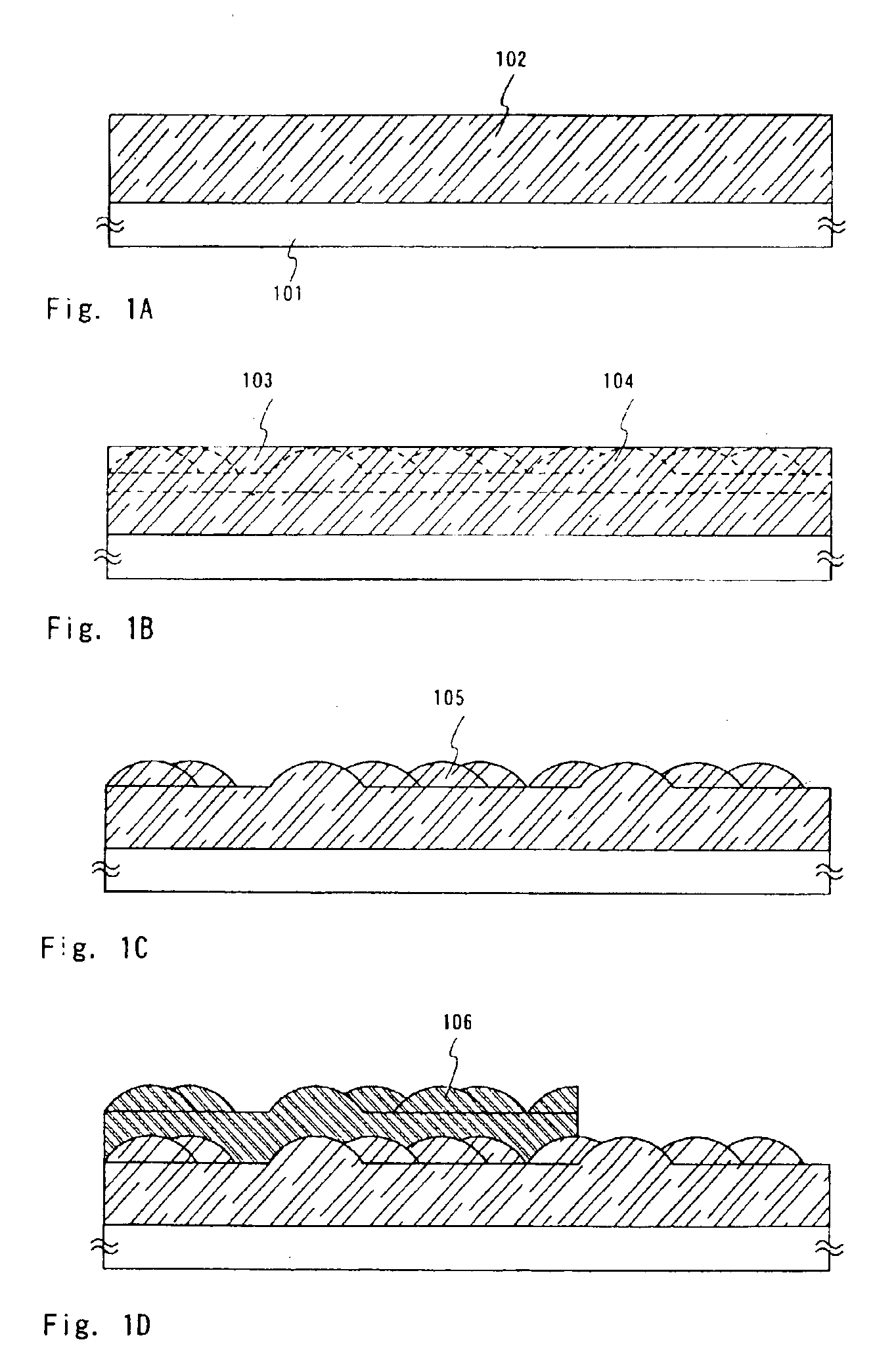
[0068]According to the example, an example of steps of fabricating an active matrix substrate having a top gate type TFT will be shown. Further, FIG. 3A through FIG. 7 showing top views and sectional views of a portion of a pixel portion will be used for explanation.

[0069]First, an amorphous semiconductor layer is formed on a substrate 301 having an insulating surface. Here, a quartz substrate is used as the substrate 301 and an amorphous semiconductor layer is formed by a film thickness of 10 through 100 nm.

[0070]Further, a glass substrate or a plastic substrate can be used other than the quartz substrate. When the glass substrate is used, the glass substrate may be subjected to a heat treatment previously at a temperature lower than a glass strain point by about 10 through 20° C. Further, a base film comprising an insulating film of a silicon oxide film, a silicon nitride film or a silicon oxynitride film may be formed on a surface of the substrate 301 for forming TFT to prevent a...

embodiment 2

[0098]In this example, a method of fabricating a transflective type liquid crystal display device having a structure different from that of Example 1 will be explained in details in reference to FIG. 8A through FIG. 10.

[0099]First, as shown by FIG. 8A, an amorphous semiconductor film is formed on a substrate 801, the amorphous semiconductor film is crystallized and thereafter, a semiconductor layer 805 separated in an island-like shape by patterning is formed. Further, a gate insulating film 806 comprising an insulating film is formed on the semiconductor layer 805. Further, a fabricating method until forming the gate insulating film 806 is similar to that shown by Example 1 and therefore, Example 1 may be referred. Further, similarly, an insulating film covering the semiconductor layer 805 is formed, thereafter, thermal oxidation is carried out and the gate insulating film 806 is formed.

[0100]Next, a channel doping step of adding a p-type and an n-type impurity element to a region ...

example 3

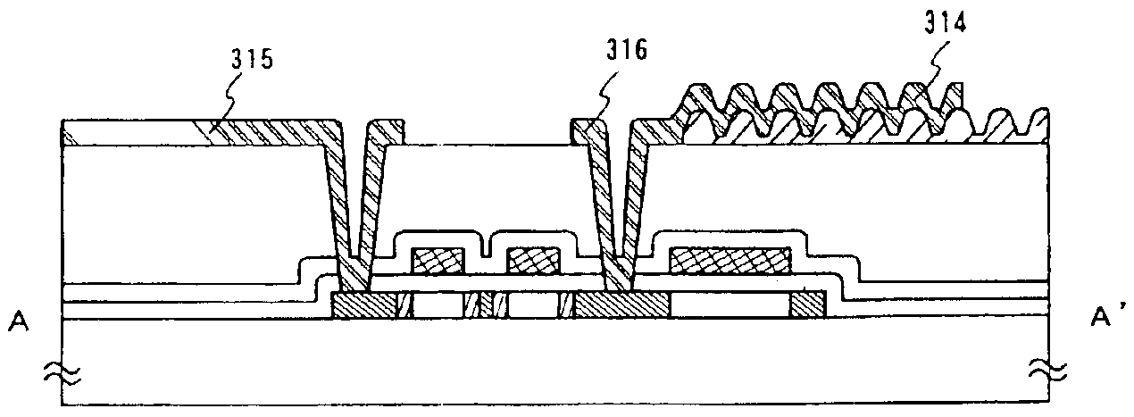
[0121]According to the example, steps of fabricating a transflective type liquid crystal display device from the active matrix substrate fabricated by Example 1 will be explained as follows. A sectional view of FIG. 11 is used for explanation.

[0122]First, after providing the active matrix substrate of FIG. 3D in accordance with the example 1, as shown by FIG. 11, an alignment film 1119 is formed on the active matrix substrate and rubbing treatment is carried out. Further, according to the example, after forming the alignment film 1119, spherical spacers 1121 for holding an interval between the substrates are scattered over entire surfaces of the substrates. Further, in place of the spherical spacers 1121, column like spacers may be formed at desired positions by patterning an organic resin film of an acrylic resin film or the like.

[0123]Next, a substrate 1122 is prepared. A coloring layer 1123 (1123a, 1123b) and a flattening layer 1124 are formed on the substrate 1122. Further, as t...


PUM

PropertyMeasurementUnit
transparentaaaaaaaaaa
wavelengthaaaaaaaaaa
reflectanceaaaaaaaaaa

Abstract

With an object of providing a transflective type liquid crystal display device having a transparent electrode of an uneven structure formed without particularly increasing steps, in fabricating the transflective type liquid crystal display device, a amorphous transparent conductive film is formed on a substrate, a crystalline portion is formed in the amorphous transparent conductive film to thereby form the transparent conductive film including the crystalline portion, a amorphous portion is removed at a film surface of the transparent conductive film including the crystalline portion to thereby form the transparent conductive film having an uneven shape formed by a remaining crystalline portion at a film surface and a reflecting electrode having the uneven shape is formed by forming a reflective conductive film above the transparent electrode having the uneven shape.

Description

BACKGROUND OF THE INVENTION[0001]1. Field of the Invention[0002]The present invention relates to liquid crystal display device of a passive matrix type and an active matrix type. Particularly, the invention relates to an electrode structure of transflective type liquid crystal display device having both functions of a transmission type and a reflection type.[0003]2. Description of the Related Art[0004]In recent years, by explosive spread of a portable information terminal represented by a portable telephone, there is needed a display capable of dealing with light-weighted formation, conservation of power consumption and a change in an environment of use.[0005]Further, in view of thin film formation and light-weighted formation, a liquid crystal display device or an organic EL display device is representatively promising.[0006]Power consumption of a transmission type display device is inconsiderable for driving only a display. However, a liquid crystal per se does not emit light and ...

Claims


Application Information

Patent Timeline
Patent Type & Authority Patents(United States)
IPC IPC(8): G02F1/1335G02F1/1343G02F1/136G02F1/1368H01L21/20H01L21/28H01L21/306H01L21/3205H01L21/336H01L23/52H01L29/786
CPCG02F1/133555G02F2001/13685G02F1/133504G02F1/13685G02F1/1335
Inventor EGUCHI, SHINGOTSUJI, YURIKO
Owner SEMICON ENERGY LAB CO LTD
Learn More