Circuit for prevention of unintentional writing to a memory, and semiconductor device equipped with said circuit

a technology for unintentional writing and memory, which is applied in the direction of unauthorized memory use protection, error detection/correction, instruments, etc., can solve the problems of inability to ensure the prescribed data holding characteristics, the non-volatile memory becomes unstable in operation, and it takes a significant amount of time to change the system back to the default setting

Active Publication Date: 2007-05-01
SEMICON COMPONENTS IND LLC
View PDF8 Cites 11 Cited by
  • Summary
  • Abstract
  • Description
  • Claims
  • Application Information

AI Technical Summary

Benefits of technology

[0012]The preferred embodiments of the present invention have been developed in view of the above-mentioned and/or other problems i...

Problems solved by technology

However, even though it is able to retain stored data when power is turned off, a nonvolatile memory becomes unstable in operation when power is first turned on or when the power supply VDD experiences transient drops in voltage.
As a result, the prescribed data holding characteristics cannot ...

Method used


Image

  • Circuit for prevention of unintentional writing to a memory, and semiconductor device equipped with said circuit
  • Circuit for prevention of unintentional writing to a memory, and semiconductor device equipped with said circuit
  • Circuit for prevention of unintentional writing to a memory, and semiconductor device equipped with said circuit

Examples


first embodiment

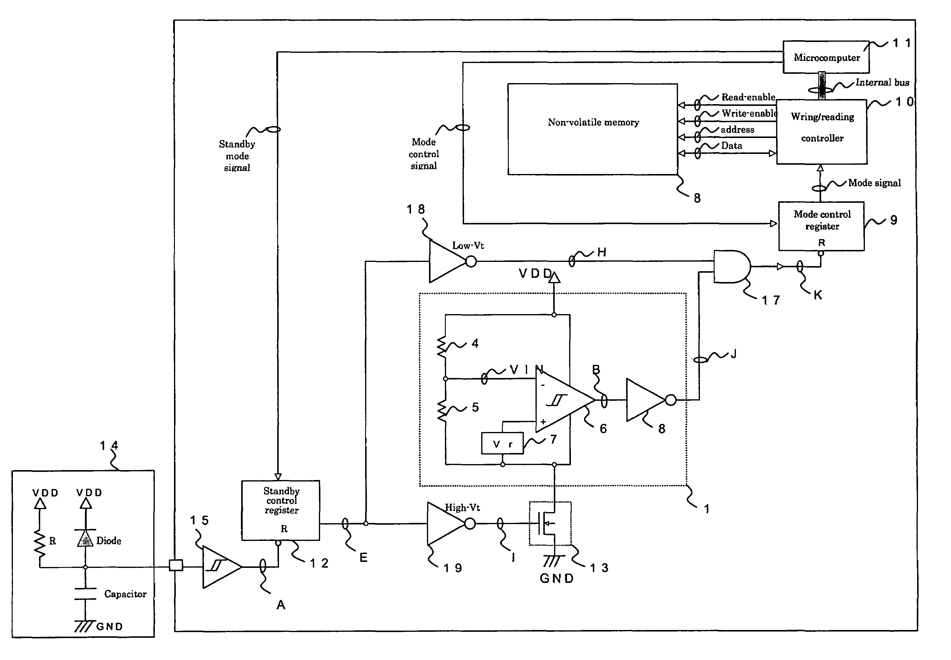
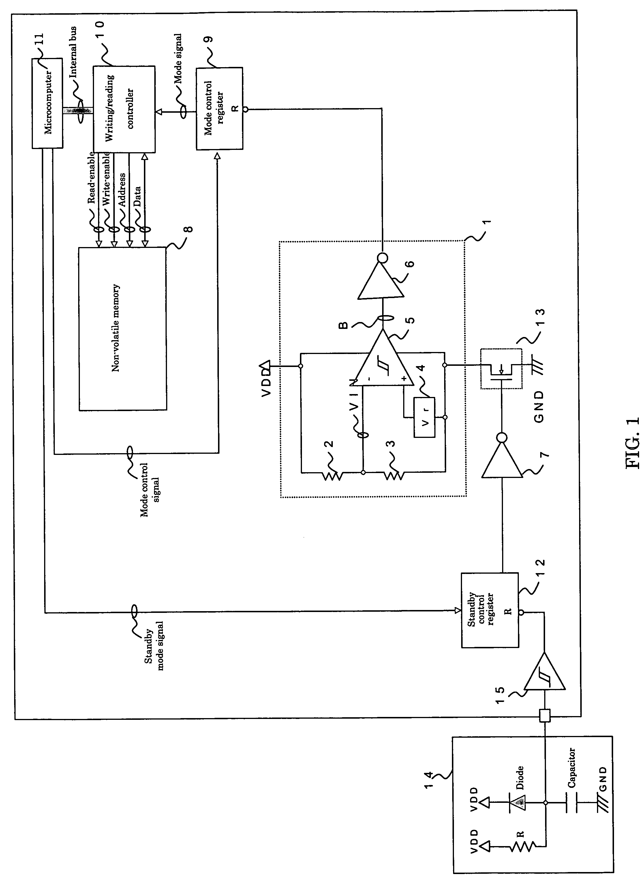
[0032]FIG. 1 shows an example of a circuit for prevention of unintentional writing to a memory according to the invention. Reference numeral “1” denotes a low-voltage detection circuit which detects a power supply voltage (VDD) drop, “2” and “3” denote resistances which divide the power supply voltage VDD, “4” denotes a reference voltage generating circuit which generates a reference value Vref as a voltage detection level, “5” denotes a comparator which compares the midpoint voltage of the resistance 2 and the resistance 3 with the reference voltage Vref, “6” denotes an inverter which inverts the output signal of the comparator 5, “7” denotes a second inverter, “8” denotes a nonvolatile memory, “9” denotes a mode control register which controls the setting of writing to and reading from the nonvolatile memory 8, and is reset by the output signal of the low-voltage detection circuit 1, “10” denotes a writing / reading controller which outputs a read-enable signal, a write-enable signa...

second embodiment

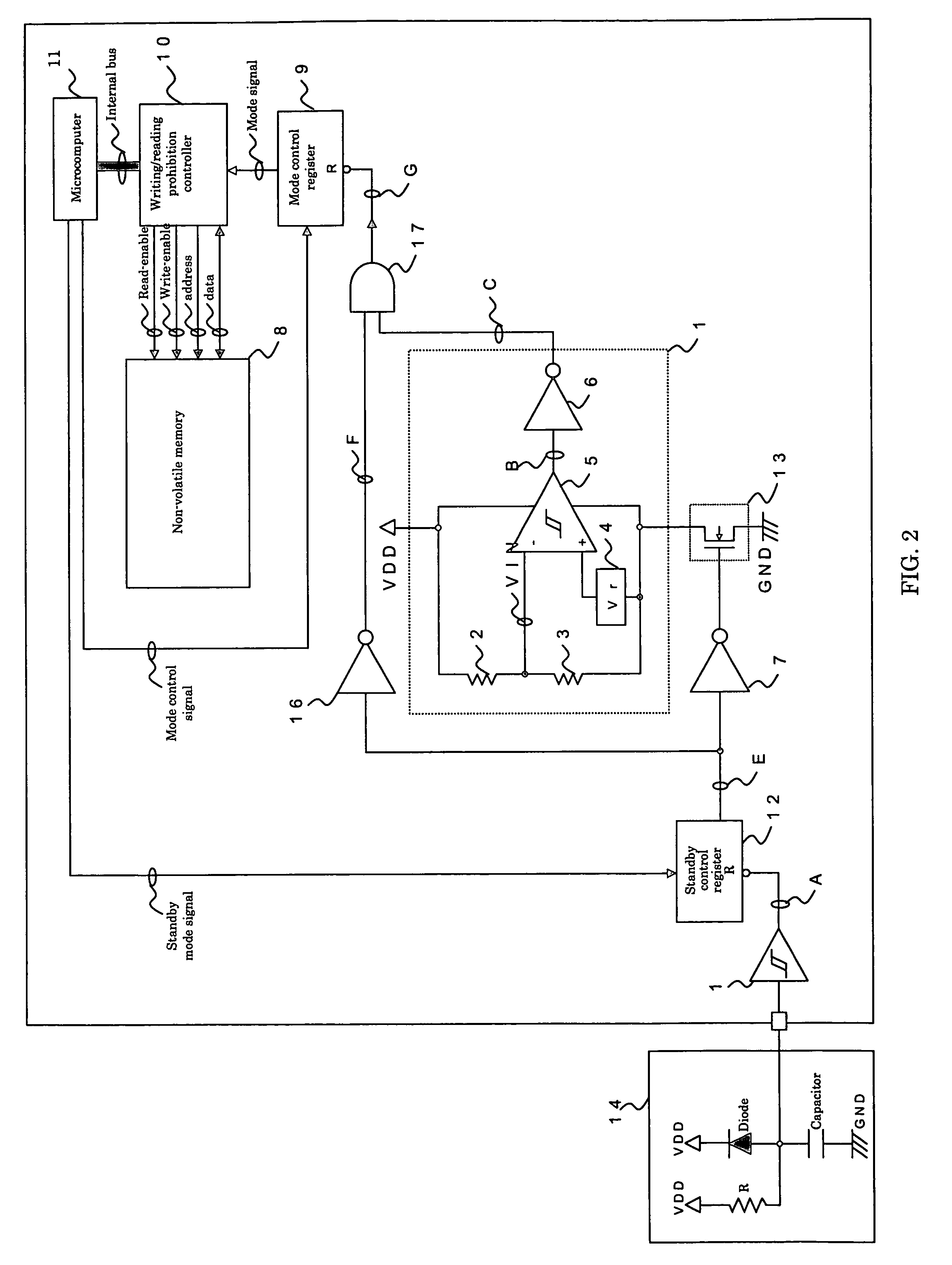
[0058]FIG. 3 is a block diagram showing a third, preferred embodiment of the present invention. This embodiment differs from the second embodiment shown in FIG. 2 in that the inverter 16 shown in FIG. 2 is replaced with a Low-Vt inverter 18 and that the inverter 7 shown in FIG. 2 is replaced with a High-Vt inverter 19. The aforementioned “Low-Vt” and “High-Vt” means a “low-threshold” and a “high-threshold,” respectively.

[0059]The Low-Vt inverter 18 becomes an “L” level at a lower input voltage because of the low-threshold as compared with an inverter having a standard threshold. Accordingly, the signal H which is an output signal of the inverter 18 is more biased to becoming an “L” level as compared with an inverter having a standard threshold and therefore more frequently outputs a reset signal to mode control register 9.

[0060]The High-Vt inverter 19 would not become an “L” level until the input voltage becomes higher because of the high-threshold as compared with an inverter havin...


PUM


Abstract

A circuit for prevention of unintentional writing to a memory prevents unintentional writing to a nonvolatile memory, after a recovery from a transitory power failure. The circuit includes a low-voltage detection circuit for detecting a power supply voltage drop depending on the state of a control signal for the detection circuit. A writing operation to the memory is prohibited depending on the control signal as well as upon an output signal of the low-voltage detection circuit.

Description

[0001]This application claims priority under 35 U.S.C. § 119 to Japanese Patent Application No. P2003-084391 filed on Mar. 26, 2003, the entire disclosure of which is incorporated herein by reference in its entirety.BACKGROUND OF THE INVENTION[0002]1. Field of the Invention[0003]The present invention relates to a circuit for prevention of unintentional writing to a memory. More specifically, it relates to a circuit equipped with a low-voltage detection circuit capable of preventing unintentional writing to a nonvolatile memory when the low-voltage detection circuit detects a drop in power supply voltage. The present invention also relates to a semiconductor device equipped with such circuit.[0004]2. Description of the Background[0005]The following description sets forth the inventor's knowledge and should not be construed as an admission that the description constitutes prior art.[0006]A nonvolatile memory, such as an EPROM, an EEPROM and a flash memory capable of erasing stored dat...

Claims


Application Information

Patent Timeline
IPC IPC(8): G06F12/14G06F11/00G11C16/02G06F13/28G06F15/78G11C16/22G11C16/34
CPCG11C16/225B42D15/02B42D15/0086
Inventor HOTAKA, KAZUO
Owner SEMICON COMPONENTS IND LLC
Why Eureka
Try Eureka