Low voltage logic circuit with set and/or reset functionality

a logic circuit and functionality technology, applied in the field of low voltage logic circuits with set and/or reset functionality, flipflops and other logic circuits, can solve the problems of scaling supply voltage, not linear, and difficult to preserve high-speed operation at low supply voltage, so as to reduce the voltage swing of differential clock signals and reduce the effect of voltage swing

Active Publication Date: 2007-05-08
CYPRESS SEMICON CORP
View PDF15 Cites 12 Cited by
  • Summary
  • Abstract
  • Description
  • Claims
  • Application Information

AI Technical Summary

Benefits of technology

[0022]In some embodiments, one or more level shift circuits may be included within the logic circuit for reducing the voltage swings of one or more signals supplied to the logic circuit. In some cases, a first level shift circuit may be included for reducing a voltage swing of the differential clock signals. As such, additional transistors may be coupled in common-emitter configurations with the first and second pairs of transistors for receiving level shifted versions of the clock and complementary clock signals, respectively. In some cases, a second level shift circuit may also be included for reducing a voltage swing of the differential SET signal or the differential RESET signal. As such, additional transistors may be coupled in common-emitter configurations with the first and second pairs of transistors for receiving a level shifted version of the SET (or RESET) signal, while another additional transistor is coupled in a common-emitter configuration with the third pair of transistors for receiving a level shifted version of the complementary SET (or complementary RESET) signal.
[0028]In some embodiments, one or more level shift circuits may be appended to the front end of the flip-flop circuit for reducing the voltage swings of one or more signals supplied thereto. In some cases, a first level shift circuit may be coupled for producing level shifted versions of the differential clock signals by reducing a voltage swing of clock and complementary clock signals supplied to the first level shift circuit. As a result, additional transistors may be coupled to the first pair of differential transistors for receiving the level shifted versions of the clock and complementary clock signals. In some cases, a second level shift circuit may also be coupled for producing level shifted versions of the differential SET or RESET signals by reducing a voltage swing of the differential SET or RESET signals supplied to the second level shift circuit. This may require even more additional transistors. For example, additional transistors may be coupled to the first pair of differential input transistors and the first pair of cross-coupled transistors for receiving the level shifted version of the SET (or RESET) signal. Yet another additional transistor may be coupled to the at least one transistor for receiving the level shifted version of the complementary SET (or complementary RESET) signal. The opposite may be true in other embodiments of the invention.

Problems solved by technology

However, it is often difficult to preserve high-speed operation at low supply voltages, especially as voltages fall below approximately 1.8 volts.
A principle difficulty in scaling the supply voltage of digital bipolar circuits (e.g., those using ECL / CML technology) is that the “turn on” potential, e.g., the base-emitter voltage (VBE) of NPN transistors, does not scale linearly with technology.
Therefore, one disadvantage of flip-flop circuit 100 is the high power supply requirement necessitated by it's two level BJT architecture.
Flip-flop circuit 100 also fails to provide SET / RESET capability, and therefore, cannot be used within circuits or devices requiring such functionality (e.g., PFD circuits).
In other words, problems may arise when input signals with CMOS voltage swings (e.g., CLK / CLKbar) are supplied to a flip-flop circuit that generates output signals with ECL / CML voltage swings (e.g., “Q” and “Qbar”).
For example, differences between input and output voltage swings may prohibit the use of auto-routing devices, which are often used for electrically connecting circuit components on a semiconductor chip.
If large CMOS voltage swings are supplied to the second stage input, they may cause the base collector junction diode to become forward biased, thereby killing the switching function of differential transistors N7 and N8.

Method used


Image

  • Low voltage logic circuit with set and/or reset functionality
  • Low voltage logic circuit with set and/or reset functionality
  • Low voltage logic circuit with set and/or reset functionality

Examples


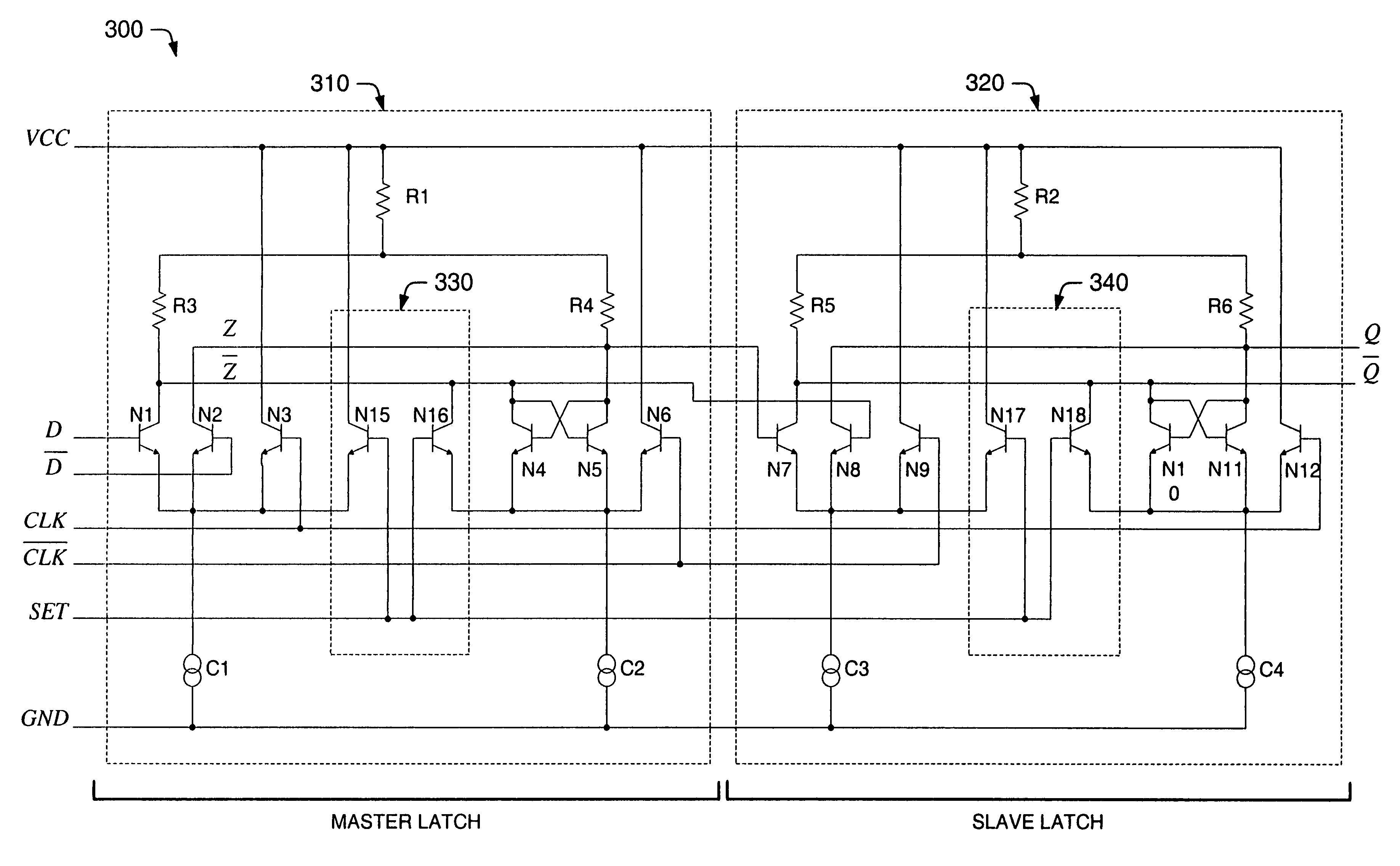
Embodiment Construction

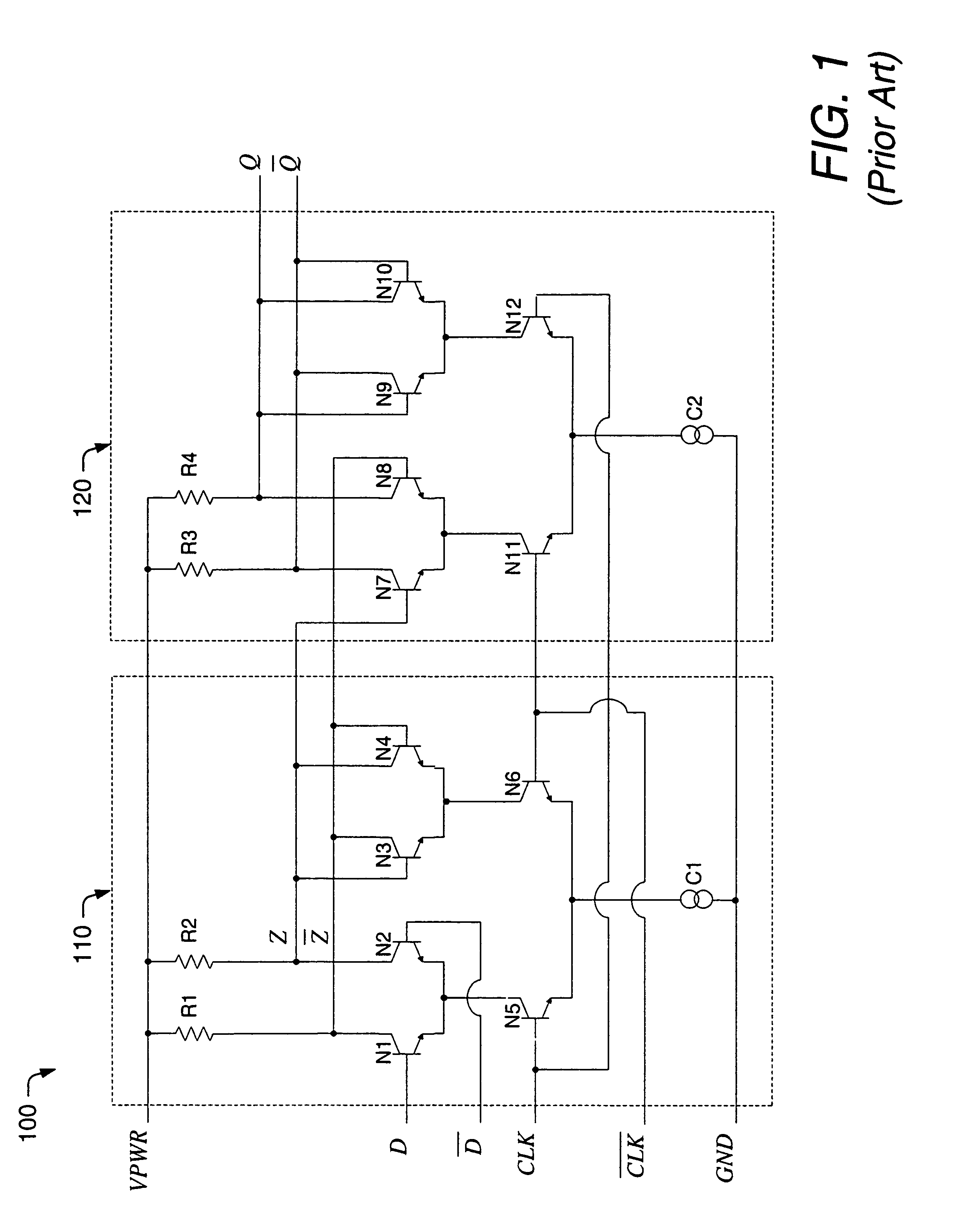
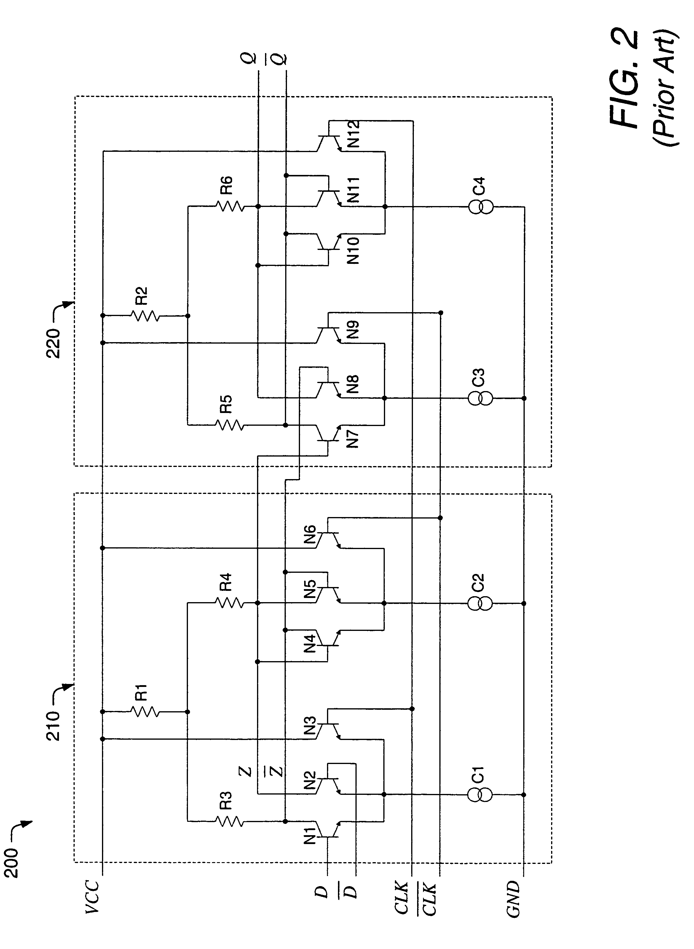
[0046]FIG. 2 illustrates another example of a conventional flip-flop circuit 200. Similar to the flip-flop circuit of FIG. 1, the current solution comprises master latch 210 and slave latch 220, each comprising six transistors. However, flip-flop circuit 200 includes no “stacked” transistors, and thus, includes no more than one base-emitter junction within any current path extending between the power supply (VCC) and ground (GND) nodes. For this reason, flip-flop circuit 200 may be generally configured for operating at relatively low supply voltages, such as those below approximately 1.8 volts. The concept of a low voltage flip-flop was first published in a paper written by Razavi, entitled “Design Techniques for Low-Voltage High-Speed Digital Bipolar Circuits,” and appearing in the IEEE Journal of Solid-State Circuits, Vol. 29, pp. 332–339, March 1994. Details of the implementation and operation of flip-flop circuit 200 may be found in the Razavi paper, which is incorporated herein...


PUM


Abstract

A low voltage logic circuit with asynchronous SET and / or RESET functions is described herein. The low voltage logic circuit may be primarily used in forming low voltage flip-flop circuits, but may also be used to form multiplexers and other logic configurations. The flip-flop circuit described herein improves upon existing low voltage architectures by providing a flip-flop circuit, which can operate at relatively low supply voltages (e.g., less than about 1.8V), with SET and / or RESET capability. In doing so, the improved flip-flop circuit may be used within a phase frequency detector, programmable counter, or frequency divider of a phase locked loop (PLL) or delay locked loop (DLL) device. However, the improved flip-flop circuit may be used with any low voltage circuit or device that may require, use or benefit from a SET or RESET function. In some embodiments, one or more level shift circuits may be included so that the low voltage flip-flop circuit may receive CML, TTL and / or CMOS logic levels (among others).

Description

PRIORITY CLAIM[0001]This application claims benefit of priority to Provisional Patent Application Ser. No. 60 / 503,225, entitled “Low Voltage CML Flip Flop for Phase Frequency Detector,” filed Sep. 16, 2003, which is hereby incorporated in its entirety.BACKGROUND OF THE INVENTION[0002]1. Field of the Invention[0003]This invention relates to electronic circuits and, more particularly, to flip-flop and other logic circuits, which are operable at low power supply voltages (e.g., less than about 1.8 volts) and have SET and / or RESET functionality.[0004]2. Description of the Related Art[0005]The following descriptions and examples are not admitted to be prior art by virtue of their inclusion within this section.[0006]Many electronic systems now use supply voltages that fall significantly below the conventional 5.0 volt standard. The demand for reduced power dissipation and battery requirements (e.g., in applications such as wireless and personal computing) has motivated designers to scale ...

Claims


Application Information

Patent Timeline
Patent Type & Authority Patents(United States)
IPC IPC(8): H03K3/00
CPCH03K3/012H03K3/289
Inventor KANG, POZENGLI, GABRIEL MING-YU
Owner CYPRESS SEMICON CORP
Why Eureka
Try Eureka