Techniques for controlling on-chip termination resistance using voltage range detection

Inactive Publication Date: 2007-05-15
ALTERA CORP
View PDF70 Cites 33 Cited by
  • Summary
  • Abstract
  • Description
  • Claims
  • Application Information

AI Technical Summary

Benefits of technology

[0007]The present invention provides techniques for controlling an on-chip termination resistance in an input or output (IO) buffer using a calibration circuit. The calibration circuit monitors the voltage between an external resistor and a group of on-chip transistors. When voltage between the external resistor and the group of transistors is within a sele

Problems solved by technology

When transmitting signals over distances that are appreciable with respect to the signal period, mismatches between the impedance of the transmission line and that of the receiver cause signal reflection.
The reflected signal interferes with the transmitted signal and causes distortion and degrades the overall signal integrity.
For many of today's high speed integ

Method used


Image

  • Techniques for controlling on-chip termination resistance using voltage range detection
  • Techniques for controlling on-chip termination resistance using voltage range detection
  • Techniques for controlling on-chip termination resistance using voltage range detection

Examples


Embodiment Construction

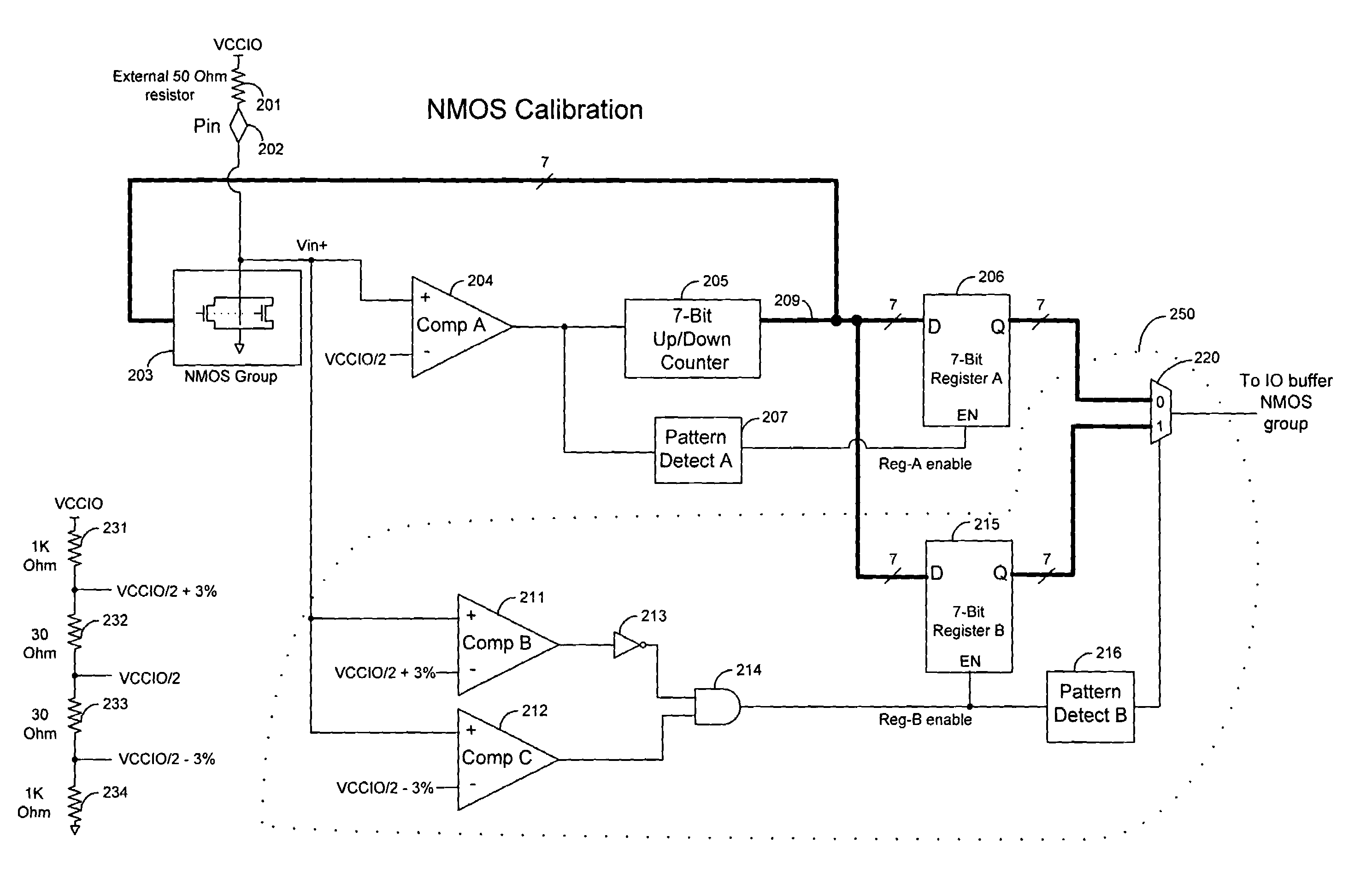
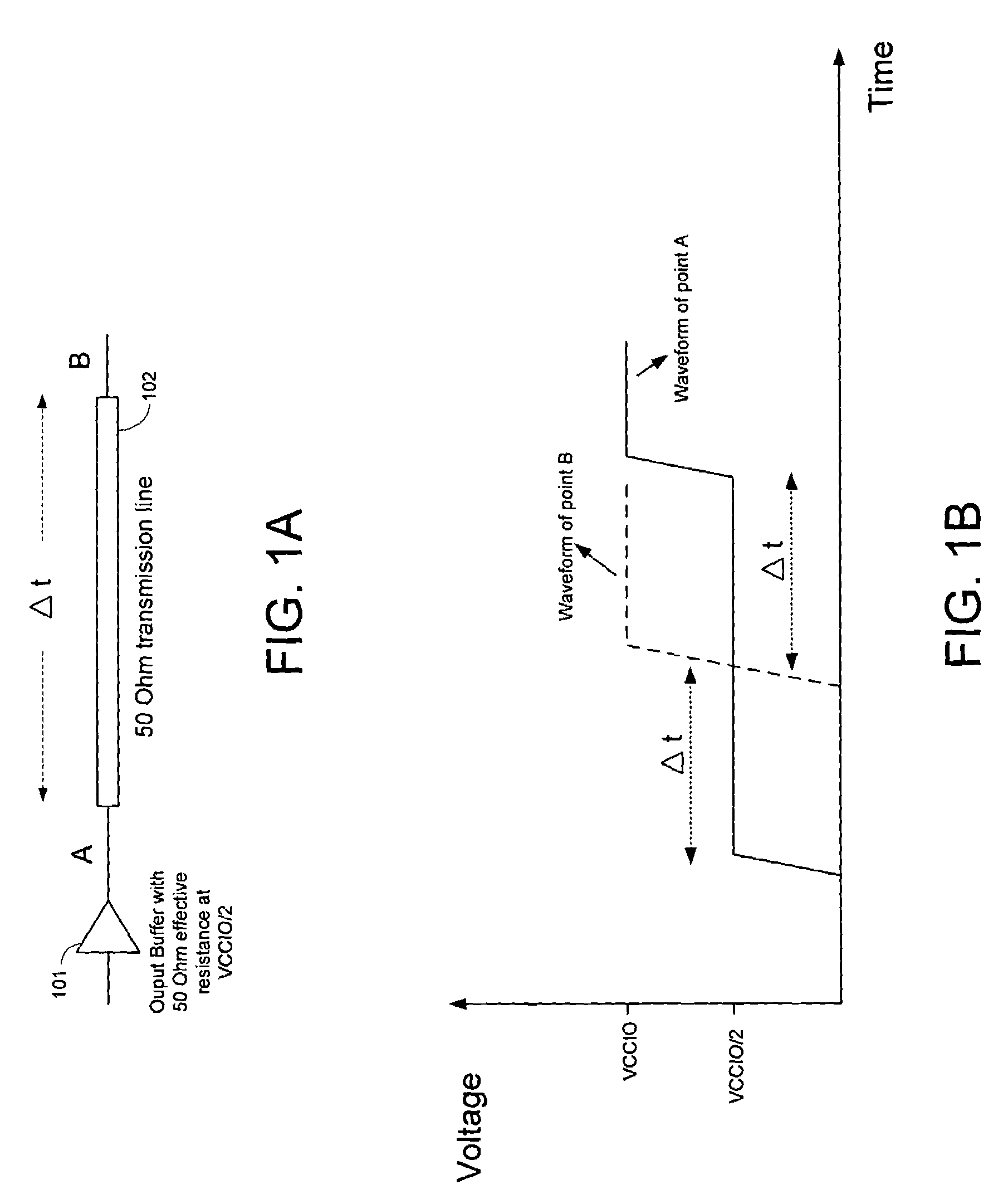
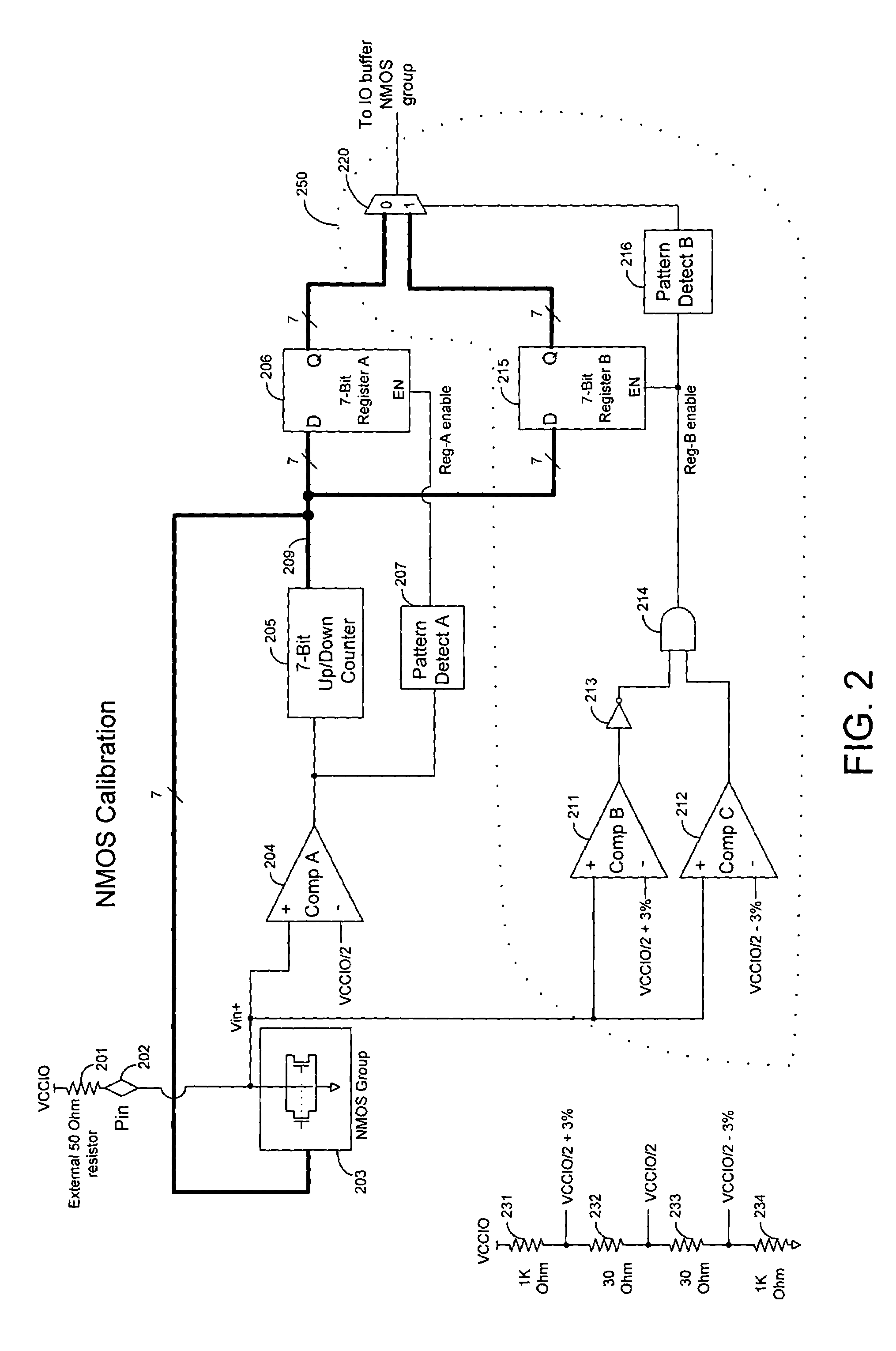
[0022]On-chip series termination can be provided by controlling the drive current strength of the output transistor(s) in an input or output (IO) buffer, to achieve a desired effective resistance. FIG. 1A illustrates an output buffer 101 coupled to drive signals on a 50 ohm transmission line 102. A signal of half the output swing travels from output buffer 101 and is reflected at an open ended transmission line 102. When the reflected waveform returns to output driver 101, the termination resistance in output buffer 101 causes the reflected signal to return to the full output voltage swing. Because the reflected signal returns to the full voltage swing, the output signal is prevented from reflecting back-and-forth in transmission line 102.

[0023]FIG. 1B shows an example of a waveform that illustrates how signals can be reflected across transmission lines. In this example, the supply voltage is VCCIO, and Δt is the time delay between points A and B on transmission line 102. As shown i...


PUM


Abstract

Techniques are provided for controlling an on-chip termination resistance in an input or output (IO) buffer using a calibration circuit. The calibration circuit monitors the voltage between an external resistor and a group of on-chip transistors. When voltage between the external resistor and the group of transistors is within a selected range, the calibration circuit causes the effective resistance of the transistors to match the resistance of the external resistor as closely as possible. The calibration circuit enables another set of transistors in the IO buffer so that the effective on resistance of the transistors in the IO buffer closely match the resistance of the external resistor.

Description

CROSS-REFERENCES TO RELATED APPLICATIONS[0001]This patent application is related to commonly-assigned, co-pending U.S. patent application Ser. No. 11 / 040,048, filed Jan. 20, 2005, which is incorporated by reference herein.BACKGROUND OF THE INVENTION[0002]The present invention relates to techniques for controlling on-chip termination resistance using voltage regulation, and more particularly, to techniques for controlling an on-chip termination resistance by monitoring an effective resistance of on-chip transistors within a selected voltage range.[0003]When transmitting signals over distances that are appreciable with respect to the signal period, mismatches between the impedance of the transmission line and that of the receiver cause signal reflection. The reflected signal interferes with the transmitted signal and causes distortion and degrades the overall signal integrity. To minimize or eliminate the unwanted reflection, transmission lines are resistively terminated by a matching...

Claims


Application Information

Patent Timeline
IPC IPC(8): H03B1/00
CPCH03K19/0005
Inventor CHANG, TZUNG-CHINWANG, XIAOBAOKIM, HENRYSUNG, CHIAKANGNGUYEN, KHAI Q.WANG, BONNIETYHACH, JEFFREYRANGAN, GOPINATH
Owner ALTERA CORP
Why Eureka
Try Eureka