Control circuitry for power gating virtual power supply rails at differing voltage potentials

a technology of virtual power supply rails and control circuits, applied in the field of complementary metal oxide semiconductor (cmos) circuits, can solve the problems of not achieving an adequate reduction in leakage power dissipation, affecting the manufacturing of small devices, and becoming a significant portion of power dissipation

Inactive Publication Date: 2007-05-15
IBM CORP
View PDF1 Cites 29 Cited by
  • Summary
  • Abstract
  • Description
  • Claims
  • Application Information

AI Technical Summary

Problems solved by technology

As CMOS circuits become smaller, leakage current that results when voltage is applied to the gate of the field effect transistors becomes a significant portion of the power dissipation.
Leakage power may become the limiting factor in how small devices may be manufactured.
However, this may not achieve an adequate reduction in leakage power dissipation.
Interfacing between circuits in a power-gated domain and circuits in a non-power-gated domain may prove difficult.
While the benefits of power-gating are known, there is no consensus on strategies to preserve logic states of outputs in the power-gated domains.
Therefore, one would expect the large devices to exhibit large gate-leakage current when the technology has gate oxides that are very thin.
Likewise, logic regions with a high number of logic gates may exhibit a large gate-leakage current due to the large number of devices that are in strong inversion at any one static time (between clock transitions).
While employing cuttable regions enables the leakage in an integrated circuit to be managed, controlling these regions may lead to significant overhead and present problems in implementing the cuttable regions.
However, if the non-power-gated domain generates control wake and sleep signals to interface with a power gated domain with a high power supply voltage, then the mismatch in voltage levels may lead to higher than desired leakage levels.
In one case, a logic one level from one domain may not adequately hold off a PFET coupled to a higher power supply voltage.
In another case, a logic zero level from one domain may not adequately hold off an NFET coupled to a higher ground potential.
Prior art techniques have distributed multiple power levels to such domains causing crowded wiring channels and increased circuit complexity.

Method used


Image

  • Control circuitry for power gating virtual power supply rails at differing voltage potentials
  • Control circuitry for power gating virtual power supply rails at differing voltage potentials
  • Control circuitry for power gating virtual power supply rails at differing voltage potentials

Examples


Embodiment Construction

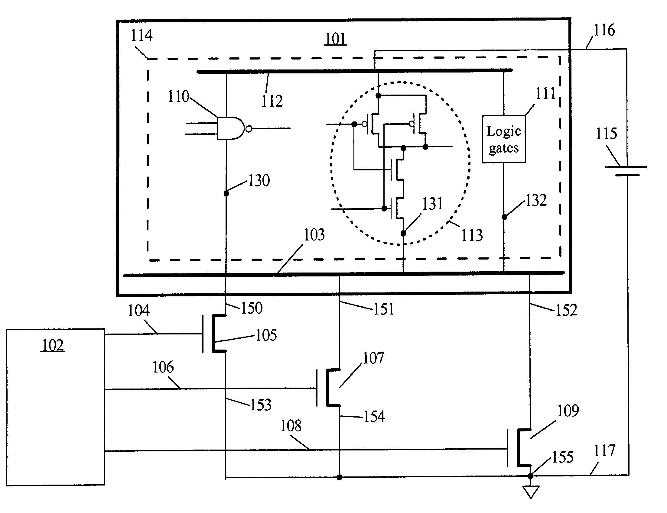
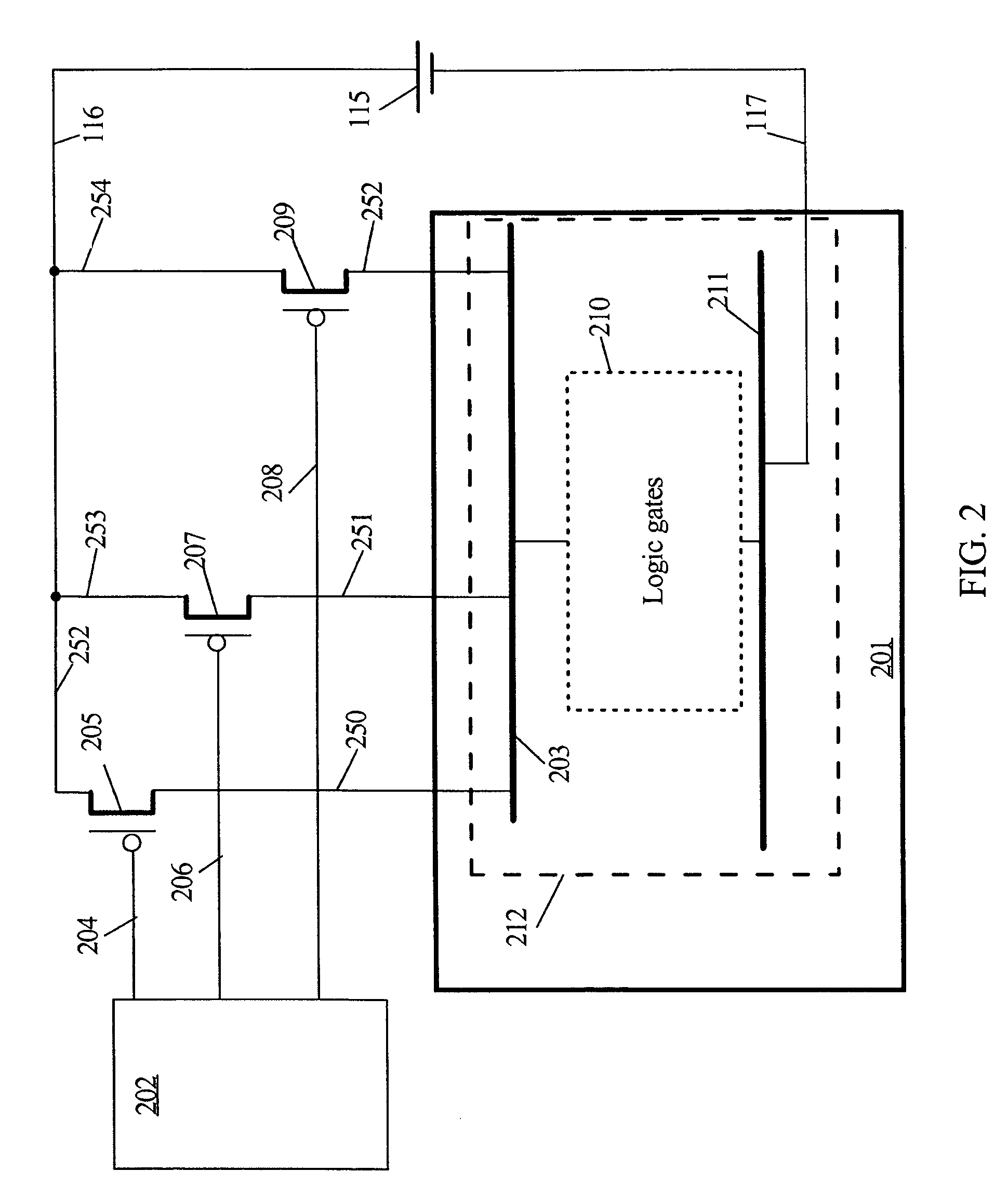
[0042]In the following description, numerous specific details are set forth to provide a thorough understanding of the present invention. However, it will be obvious to those skilled in the art that the present invention may be practiced without such specific details. In other instances, well-known circuits may be shown in block diagram form in order not to obscure the present invention in unnecessary detail. For the most part, details concerning timing, and the like have been omitted inasmuch as such details are not necessary to obtain a complete understanding of the present invention and are within the skills of persons of ordinary skill in the relevant art.

[0043]In the following, power supply voltage potentials are distributed to circuits on circuit traces or printed wires which may be referred to interchangeably as power supply rails, grids or buses. Power supply voltage potentials are coupled to the buses or grids to activate various logic circuitry. The power supply voltage po...


PUM


Abstract

A single-stage level shifting circuit is used to interface control signals across the boundary between voltage domains with differing positive or ground voltage potentials Asserted states are determined by the difference between the positive voltages potentials and the ground potentials. A lower positive power supply potential is not used to turn OFF PFET coupled to a higher positive power supply potential. Likewise a higher ground power supply potential is not used to turn OF NFETs coupled to a power domain where is significant ground shift. The single stage level shifting circuit has keeper devices that hold asserted states using voltages within the power gated domain.

Description

GOVERNMENT RIGHTS[0001]This invention was made with Government support under NBCH30390004, BGR W0132280 awarded by PERCS II. The Government has certain rights in this invention.CROSS-REFERENCE TO RELATED APPLICATIONS[0002]The present invention is related to U.S. patent application Ser. No. 10 / 821,047, filed Apr. 8, 2004, entitled “AN INTERFACE CIRCUIT FOR COUPLING BETWEEN LOGIC CIRCUIT DOMAINS,”[0003]U.S. patent application Ser. No. 10 / 926,597, filed Aug. 26, 2004 entitled “A POWER-GATING CELL FOR VIRTUAL POWER RAILS,”[0004]U.S. patent application Ser. No. 10 / 821,048, filed Apr. 8, 2004, entitled “BUFFER / DRIVER CIRCUITS,” and[0005]U.S. patent application Ser. No. 10 / 835,501, filed Apr. 29, 2004, entitled “SELF LIMITING GATE LEAKAGE DRIVER,” which are incorporated by reference herein.TECHNICAL FIELD[0006]The present invention relates in general to complementary metal oxide semiconductor (CMOS) circuits and, in particular, to circuit methodologies for implementing power-gating to cont...

Claims


Application Information

Patent Timeline
Patent Type & Authority Patents(United States)
IPC IPC(8): G06F1/32G05F1/10
CPCH03K19/0016
Inventor KUANG, JENTE BENEDICTNGO, HUNG C.NOWKA, KEVIN JOHN
Owner IBM CORP
Why Eureka
Try Eureka