Semiconductor device and programming method

a technology of semiconductors and memory cells, applied in the field of semiconductor devices and programming methods, can solve problems such as the application of programming stress, and achieve the effects of increasing the number of bits to be programmed simultaneously, maintaining constant voltage drop, and constant programming level of data to be programmed into memory cells

Active Publication Date: 2007-05-22
MONTEREY RES LLC
View PDF9 Cites 20 Cited by
  • Summary
  • Abstract
  • Description
  • Claims
  • Application Information

AI Technical Summary

Benefits of technology

[0011]According to an aspect of the present invention, preferably, there is provided a semiconductor device including: word lines; bit lines; non-volatile memory cells connected to the word lines and the bit lines, pages being defined for each of the word lines, each of the pages having a given number of non-volatile memory cells; and a select and write circuit selecting pages that are not adjacent to each other and simultaneously programming memory cells of the pages thus selected. The stress caused by programming is not applied to the memory cells that are not to be programmed, by increasing a distance between the memory cells that are programmed simultaneously.
[0013]On the above-mentioned semiconductor device, the select and write circuit may set bit lines connected to memory cells of pages that are not programmed to a floating state. The bit lines of the memory cells into which the data is not programmed are set to the floating state. This prevents the cell current flowing the memory cells into which the data is not programmed through the bit line. Thus, there does not arise a problem in that an unnecessary data is programmed or the stress is applied to the memory cell.
[0016]The semiconductor device may further include a high-voltage generating circuit generating a high voltage for programming the non-volatile memory cells; and a selector circuit selecting the high voltage generated by the high-voltage generating circuit in the first mode and selecting another high voltage applied from an outside of the semiconductor device in the second mode, a selected high voltage being supplied to the select and write circuit. The programming mode changes from where the high voltage is supplied, and the programming mode that cannot be achieved with an internal high-voltage generating circuit can be available. Thus, the number of bits to be programmed simultaneously can be increased.
[0018]On the semiconductor device, the programming level equalizing circuit may include programming level equalizing sub-circuits; and each of the programming level equalizing sub-circuits is provided to a respective pair of two adjacent pages that are not simultaneously programmed. The voltage drop can be kept constant at the time of programming the data, by flowing the current substantially equal to the cell current across the programming level equalizing circuit. The cell current flows from the selected bit line to the memory cell. Thus, the data programming level to be programmed in the memory cell can be kept constant. The programming level equalizing circuit can be shared by the adjacent two pages in which the data is not programmed simultaneously. Thus, the number of circuits can be reduced, and the device configuration can be scaled down.
[0021]According to an aspect of the present invention, preferably, there is provided a method of programming non-volatile memory cells, including the steps of: selecting pages that are not adjacent to each other in which the pages thus selected being related to one word line, and each of the pages has a given number of non-volatile memory cells; and simultaneously programming memory cells of the pages selected. An unnecessary stress caused by programming is not applied to the memory cell into which the programming is not performed by increasing the distance between the memory cells to be programmed simultaneously.
[0023]The method may further include a step of setting bit lines connected to memory cells of pages that are not programmed to a floating state. The floating state is set to the bit line of the memory cell of the page into which the data is not programmed. This can prevent the cell current flowing across the memory cell into which the data is not programmed through the bit line. Thus, there doesn't arise a problem in that an unnecessary data is not programmed in the memory cell or the stress is applied to the memory cell.

Problems solved by technology

If a distance is too short between the memory cells in which multiple bits are programmed simultaneously, there arises a problem in that a stress caused by programming is applied to other memory cells in which nothing is to be programmed.

Method used


Image

  • Semiconductor device and programming method
  • Semiconductor device and programming method
  • Semiconductor device and programming method

Examples


Embodiment Construction

[0035]A description will now be given, with reference to the accompanying drawings, of embodiments of the present invention.

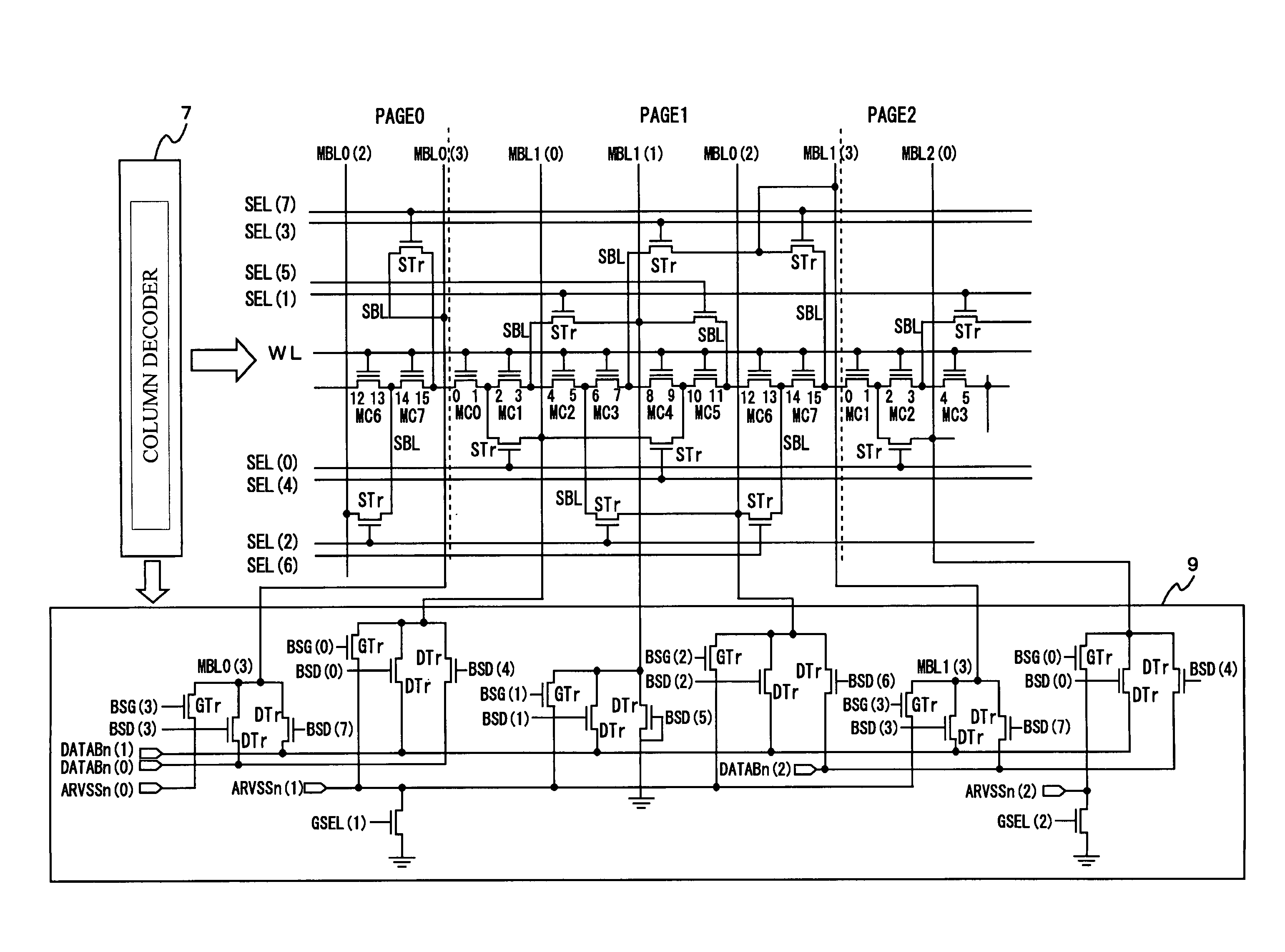
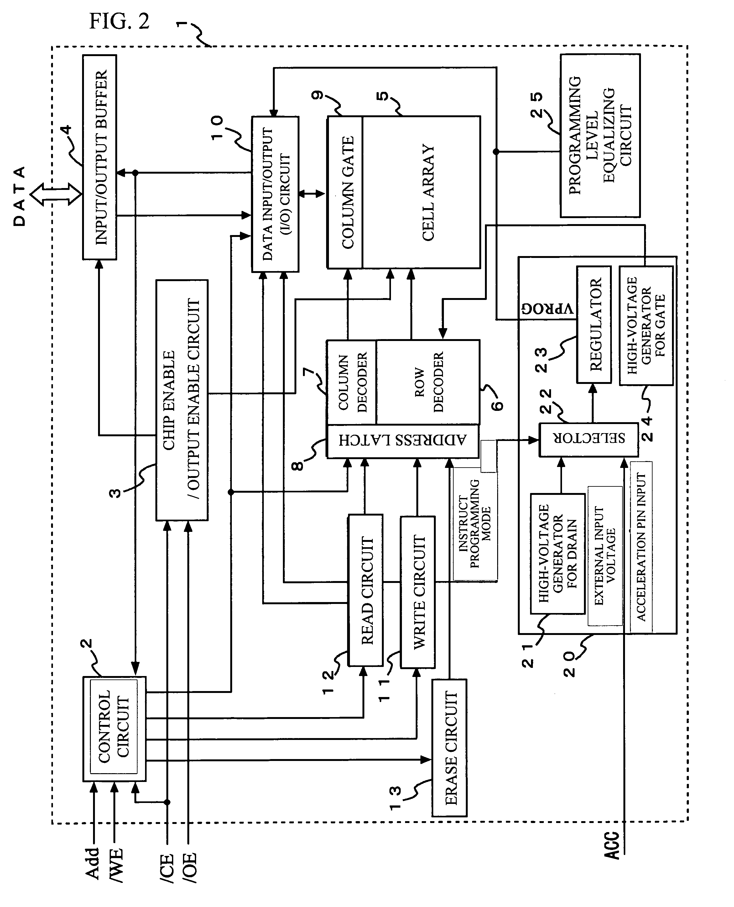
[0036]FIG. 2 shows a configuration of a semiconductor in accordance with an embodiment of the present invention. The semiconductor device in FIG. 2 is an embodiment of a non-volatile semiconductor memory device 1 including a control circuit 2, a chip enable / output enable circuit 3, an input / output buffer 4, a cell array 5, a row decoder 6, a column decoder (select and write means) 7, an address latch 8, a column gate 9, a data input / output circuit (I / O) 10, a write circuit 11, a read circuit 12, an erase circuit 13, and a power supply 20. The power supply 20 includes a high-voltage generator 21 for drain, a selector 22, a regulator 23, and a high-voltage generator for gate 24.

[0037]The control circuit 2 receives control signals such as a write enable ( / WE) and a chip enable ( / CE), an address signal, and a data signal from the outside, and serves as a state mach...


PUM


Abstract

The semiconductor device of the present invention includes a column decoder (select and write circuit), which selects multiple pages that are not located adjacently to each other so as to simultaneously program multiple bits in the memory cells of the selected page, when the multiple bits are programmed in the multiple pages. The page is a selection unit and is composed of a given number of the memory cells located on a same word line. An unnecessary stress of programming is not applied to the memory cells that are not to be programmed, by increasing the distance between the memory cells to be programmed simultaneously.

Description

CROSS REFERENCE TO RELATED APPLICATIONS[0001]This is a continuation of International Application No. PCT / JP2004 / 006263, filed May 11, 2004.BACKGROUND OF THE INVENTION[0002]1. Field of the Invention[0003]The present invention relates to a semiconductor device in which multiple bits of data can be programmed and a programming method thereof.[0004]2. Description of the Related Art[0005]The semiconductor device such as a non-volatile semiconductor device is designed to have a large capacity with the advancements of the processing technology. Programming and erasing are increasingly demanded to be faster in accordance with the large capacity of the semiconductor device.[0006]In a flash memory, all the bits have to be programmed before erasing, and so an increase in the programming speed increases the erasing speed. This is because multiple data are programmed by one byte (eight bits) or one word (16 bits) simultaneously.[0007]However, adjacent memory cells on the same word line share the...

Claims


Application Information

Patent Timeline
Patent Type & Authority Patents(United States)
IPC IPC(8): G11C11/34G11C16/04G11C16/10G11C16/12
CPCG11C16/12G11C16/10
Inventor YAMASHITA, MINORUKURIHARA, KAZUHIROWADA, HIROAKI
Owner MONTEREY RES LLC
Why Eureka
Try Eureka