OLED display and touch screen

a technology of light-emitting diodes and display screens, which is applied in the field of organic light-emitting diodes (oled) displays, can solve the problems of increasing the cost of display and touch screen redundant components, increasing the weight of the device, and the use of frames, so as to reduce the weight, size and cost, and improve the sensitivity and resolution. , the effect of reducing the size and cos

Active Publication Date: 2007-06-12
GLOBAL OLED TECH
View PDF3 Cites 124 Cited by
  • Summary
  • Abstract
  • Description
  • Claims
  • Application Information

AI Technical Summary

Benefits of technology

[0007]The display according to the present invention is advantageous in that it provides a thin, light, easily manufacturable display having an integrated optical touch screen having reduced weight, size, and cost, a greater reliability and improved sensitivity and resolution.

Problems solved by technology

These prior-art arrangements combining touch screens and OLED displays suffer from a variety of drawbacks.
The use of frames increases the parts count, weight, and cost of the device.
Redundant components found in the display and touch screen further increase cost and decrease performance as compared to more integrated solutions.
Moreover, the need for separate cabling for the touch screen increases manufacturing costs.
While advantageous, sensors employed in such an arrangement may not provide sufficient sensitivity and resolution to meet needs for some applications.

Method used


Image

  • OLED display and touch screen
  • OLED display and touch screen
  • OLED display and touch screen

Examples


Embodiment Construction

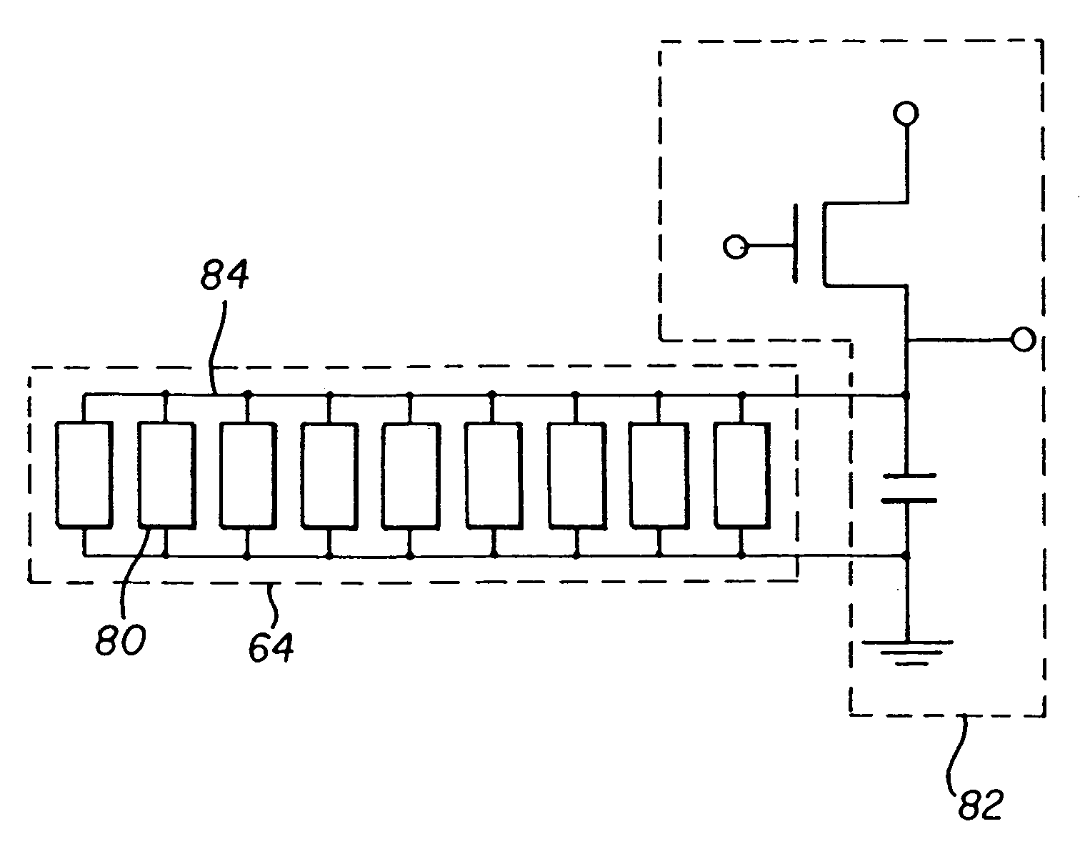
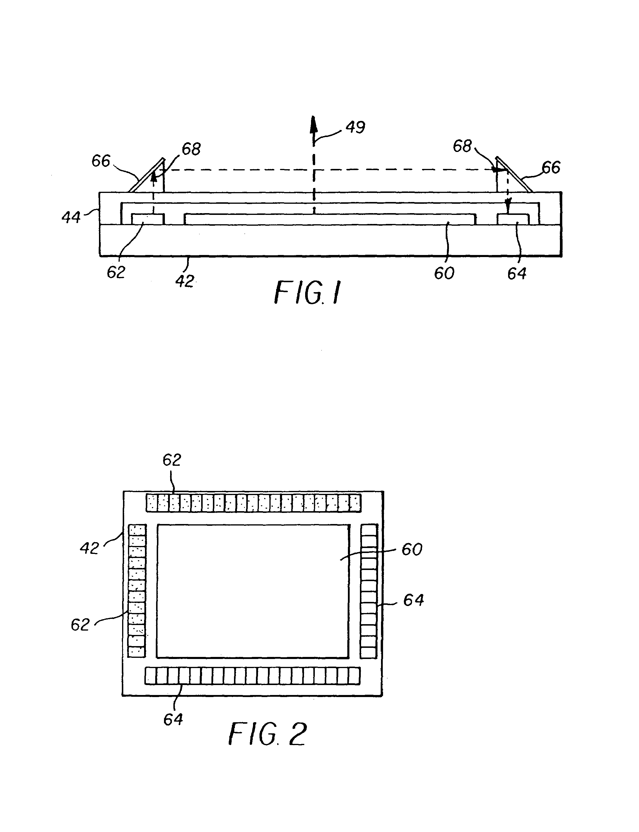
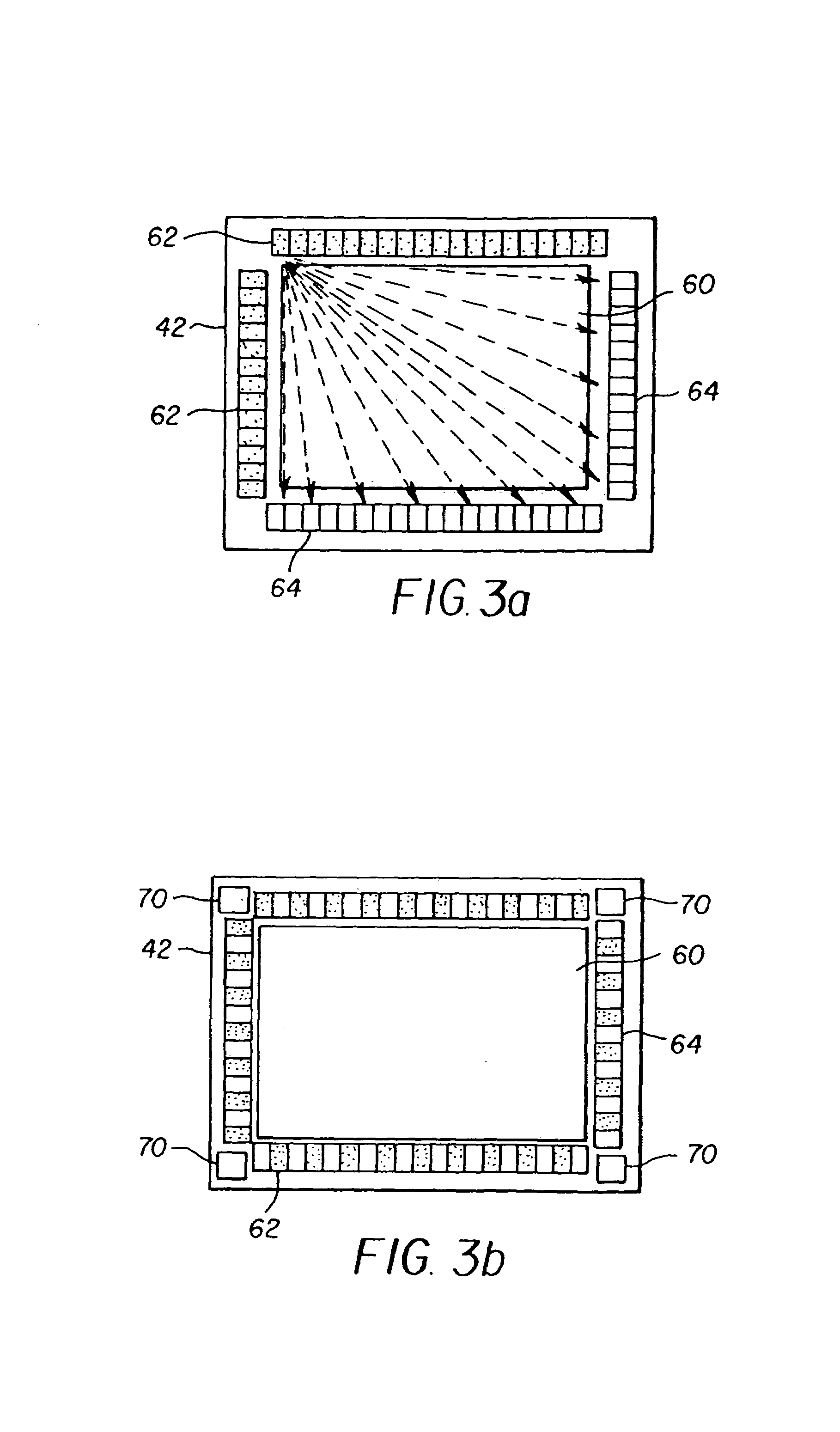
[0013]Referring to FIG. 1, a top-emitting OLED display device with an integrated optical touch screen according to one embodiment of the present invention includes a rectangular substrate 42 with an encapsulating cover 44. Located on the substrate is an OLED display area 60 including electrodes and multiple layers of materials such as hole-injection layers and electron transport layers as is well known in the art (not shown), which make up an array of individually addressable OLEDs formed on the substrate. Light 49 emitted from the display passes through the encapsulating cover 44 or is reflected from the substrate 42 and is emitted through the encapsulating cover 44. At one side of the substrate 42 is an array of infra-red OLED light emitters 62 adjacent to an edge of the display area 60. Infrared OLED light emitters are known and can be made, for example, by doping OLED devices with rare-earth ions such as neodymium or erbium. At the opposite side of the rectangular substrate 42, ...


PUM


Abstract

An OLED display and touch screen system, including: a) a substrate; b) an OLED display area including an array of individually addressable OLEDs formed on the substrate; and c) a touch screen including at least one OLED light emitter formed on the substrate and a plurality of light sensors formed on the substrate across the display area from the light emitter, each of the light sensors having an elongated surface area with a first relatively short dimension and a second relatively long dimension and being positioned adjacent to an edge of the display area, with the relatively long dimension positioned substantially perpendicular to the adjacent edge of the display area, and optics located around the display area above the light emitter and the light sensors for directing light emitted from the light emitter across the display area to the surface area of the light sensors. The system is advantageous in that it enables a thin, light, easily manufacturable display having an integrated optical touch screen having reduced weight, size, and cost, a greater reliability and improved sensitivity and resolution.

Description

FIELD OF THE INVENTION[0001]This invention relates generally to organic light emitting diode (OLED) displays and, more particularly, to an OLED display with a touch screen.BACKGROUND OF THE INVENTION[0002]Modern electronic devices provide an increasing amount of functionality with a decreasing size. By continually integrating more and more capabilities within electronic devices, costs are reduced and reliability increased. Touch screens are frequently used in combination with conventional soft displays such as cathode ray tubes (CRTs), liquid crystal displays (LCDs), plasma displays and electroluminescent displays. The touch screens are manufactured as separate devices and mechanically mated to the viewing surfaces of the displays.[0003]U.S. 2002 / 0175900 A1 by Armstrong, published Nov. 28, 2002, describes a touch system for use with an information display system including a frame defining an opening corresponding in size and shape to an information display area of a display. On each...

Claims


Application Information

Patent Timeline
Patent Type & Authority Patents(United States)
IPC IPC(8): G09G5/00G06F3/042G09G3/32
CPCG06F3/0421G09G3/3208G09G2320/0626G09G2360/144
Inventor COK, RONALD S.
Owner GLOBAL OLED TECH
Why Eureka
Try Eureka