Integrated data jitter generator for the testing of high-speed serial interfaces

Active Publication Date: 2007-06-12
STMICROELECTRONICS SRL
View PDF11 Cites 21 Cited by
  • Summary
  • Abstract
  • Description
  • Claims
  • Application Information

AI Technical Summary

Benefits of technology

[0013]According to the present invention, a convenient jitter testing ability is provided by adding a high-speed modulation command in the transmitter data path of a serial interface. The added high-speed modulation command has a minimal co

Problems solved by technology

Electronic thermal noise, circuit timing dependence on supply voltage noise, and electromagnetic coupling are some of the sources of this jitter.
Measuring the receiver jitter tolerance has been one of the more demanding measurements due to the equipment required to produce a data stream with known amounts and frequencies of jitter.
The equipment currently available for such testing is quite expensive and the availability sometimes lags the need for testing the data link.
This is difficult to accomplish and prone to errors when using the present jittered data generation equipment such as serial dat

Method used


Image

  • Integrated data jitter generator for the testing of high-speed serial interfaces
  • Integrated data jitter generator for the testing of high-speed serial interfaces
  • Integrated data jitter generator for the testing of high-speed serial interfaces

Examples


Embodiment Construction

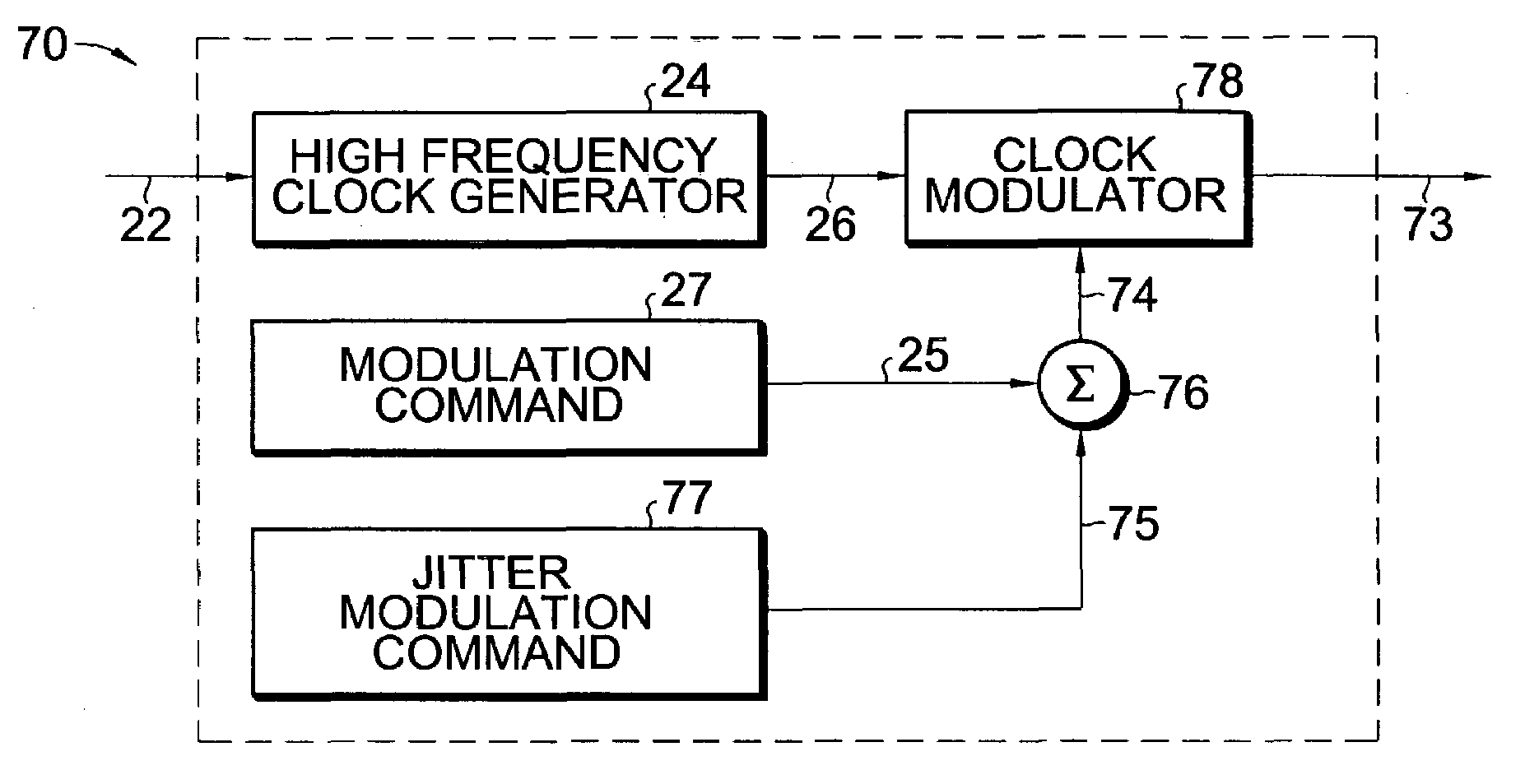
[0019]Referring now to FIG. 7, a transmit timing generation block 70 is shown according to the present invention corresponding to the previous prior art transmit timing generation block 20 shown in FIG. 2. Timing generation block 70 processes a base frequency clock signal 22 and generates a modulated high frequency clock signal 73 as a timing signal for transmitting serial data suitable for downstream jitter testing.

[0020]In the transmit timing generation block 70, the high frequency clock generator 24 increases the frequency of the base frequency clock signal to a higher fixed frequency value required by the serializer block 13 (shown in FIG. 1 but not shown in FIG. 7) to convert the parallel data to serial transmit data at the desired data rate. The modified clock modulator 78 can be implemented with variable delays (i.e. a variable delay generator). The modification to the clock modulator 78, over that of the prior art, can include increases in the range and increment resolution ...


PUM


Abstract

An integrated data jitter generator for the testing of high speed serial interfaces is provided. A transmit timing generator for use in a transmit data path includes a high frequency clock generator such as a phase-locked loop or a delay-locked loop having an input for receiving an oscillator or reference clock input. A clock modulator receives both an existing low frequency modulation signal and a high frequency modulation signal. A high-speed modulated clock signal is generated to enable jitter testing by a downstream-coupled receiver. Fixed frequencies such as 3, 6, 125, 150, 250, 300, 750, or 1500 MHz are used for the high-speed modulation signal, but any high-speed modulation frequency can be used to generate the desired amount of jitter. Likewise, the amplitude of the high frequency modulation signal can also be varied as desired.

Description

BACKGROUND OF THE INVENTION[0001]This invention pertains to high-speed serial interfaces, and, more particularly, to an apparatus and method for injecting controlled amounts and frequencies of timing jitter into the transmit data path of a serial data interface to allow for the convenient testing of jitter tolerance.[0002]In serial interfaces, several parameters of the transmitter and receiver influence the capability of the serial data link to provide data with a very low number of errors over time. This description of the number of errors per number of data bits transferred is known as the “BER” or Bit Error Rate. One of these parameters is known as “receiver jitter tolerance”. In high-speed electronic data systems, the parameter “jitter” or “timing jitter” refers to errors in the placement of a data or clock edge compared to its ideal location. The error can be random in nature or deterministic (having a bounded amplitude). The type of jitter depends on the sources of the jitter ...

Claims


Application Information

Patent Timeline
IPC IPC(8): H04B3/46G06F13/00G01R31/317H03K5/156H04L1/20H04L27/12
CPCG01R31/31709H04L1/205G01R31/31715
Inventor HILL, JOHN P.
Owner STMICROELECTRONICS SRL
Why Eureka
Try Eureka