Method and system for inspecting electronic circuit pattern

a technology of electronic circuit and pattern, applied in the direction of material analysis using wave/particle radiation, semiconductor/solid-state device testing/measurement, instruments, etc., can solve the problem of large difference in signal intensity between the defect portion and the normal portion in an image, false report, and the defect that is smaller than the noise removal threshold value cannot be detected, so as to improve the efficiency of setting the partial inspection area

Inactive Publication Date: 2007-06-12
HITACHI LTD
View PDF4 Cites 47 Cited by
  • Summary
  • Abstract
  • Description
  • Claims
  • Application Information

AI Technical Summary

Benefits of technology

[0035]The present invention provides a defect-inspection control system for inspecting an electronic circuit pattern, a defect inspecting system and an apparatus for inspecting an electronic circuit pattern, which

Problems solved by technology

This is because as regards a difference image between the reference image and the defect image, brightness distribution of a normal portion tends to decrease, as they get nearer physically, which results in a large difference in signal intensity between the defect portion and the normal portion in an image.
Usually, detection of a component except such a defect area causes a false report.
This means that the defect that is smaller than a noise removal threshold value cannot be detected.
If there are more false reports than expected, this means that sensitivity is too high.
As described as the prior art, including selection which method should be executed (the cell comparison method or the die comparison method), concerning general inspection parameters, even if the operator tries to divide an area to be inspected into many partial inspection areas, and tries to set a different inspection parameter for each partial inspection area, setting of each partial inspection area is forced to depend on manpower, which hinders efficient setting.
Division by manual operation into many partial inspection areas of which an inspection parameter is different substantially, and an inspection by manual setting the inspection parameter which is different for each partial inspection area, become impossible substantially.
This is disadvantageous in t

Method used


Image

  • Method and system for inspecting electronic circuit pattern
  • Method and system for inspecting electronic circuit pattern
  • Method and system for inspecting electronic circuit pattern

Examples


first embodiment

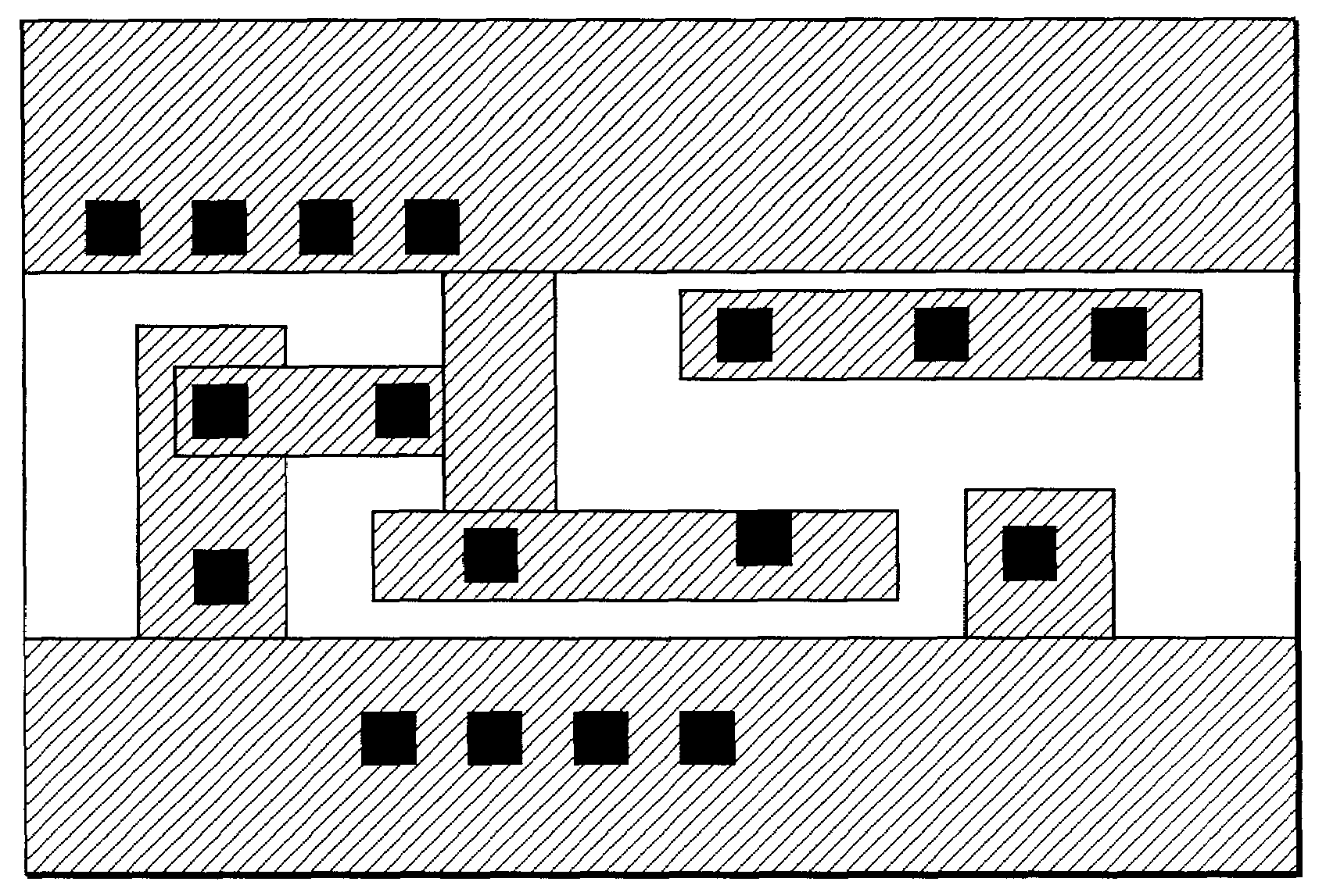
[0073]FIG. 1 is a configuration diagram illustrating a defect-inspection control system for inspecting an electronic circuit pattern according to the present invention. Reference numeral 1 denotes a pattern inspecting apparatus; 2 denotes a design information server; and 3 denotes a network such as LAN.

[0074]In the figure, the pattern inspecting apparatus 1 is connected to the design information server 2 through the network 3, which permits data to be transmitted to and received from the design information server 2. The design information server 2 stores the layout data of a semiconductor wafer to be inspected. The pattern inspecting apparatus 1 divides an area to be inspected on a chip in the semiconductor wafer into each of function blocks (for example a cell portion and non-cell portions) on the basis of the layout data 29, provides a database of inspection parameters 40 and decides inspection parameters (inspection conditions are consisted from condition of optical system and co...

second embodiment

[0092]FIG. 5 is a configuration diagram illustrating a defect-inspection control system for inspecting an electronic circuit pattern, according to the present invention. Reference numeral 8 denotes a defect reviewing apparatus. Similar reference numerals have been used for similar parts corresponding to FIG. 1. Therefore, repeated description will be omitted.

[0093]In the figure, in the second embodiment, in addition to the configuration shown in FIG. 1, the defect reviewing apparatus 8 is connected to a LAN 3, which permits data to be transmitted and received between the pattern inspecting apparatus 1 and the design information server 2. Additionally, the design information server 2 stores design information for each kind of products to be inspected and for each process of the products to be inspected.

[0094]Targeting a wafer, on which a position of a defect is already known, the defect reviewing apparatus 8 detects an image again at the defect position for the purpose of observing t...

third embodiment

[0102]Next, a defect-inspection control system for inspecting an electronic circuit pattern according to the present invention will be described.

[0103]The third embodiment also has a configuration as shown in FIG. 5. However, in addition to it, the third embodiment enables flexible adjustment of a partial inspection area as compared with the first and the second embodiment described above. In the first and the second embodiment, in order to perform completely automatic setting of a partial inspection area according to layout data, flexible adjustment of the partial inspection area is not always possible. In the third embodiment, a defect position, which has been detected by the pattern inspecting apparatus, is reviewed by the defect reviewing apparatus. After that, review results are given to inspection parameter setting of the pattern inspecting apparatus as feedback.

[0104]More specifically, the position of the defect, which has been detected by the pattern inspecting apparatus 1 i...


PUM


Abstract

For the purpose of reducing a false report and shortening inspection time, an area to be inspected is locally inspected under optimum inspection conditions. In order to avoid the number of detected defects from increasing explosively, and thereby to facilitate control of a critical defect, general-purpose layout data, which is used for producing a mask of a semiconductor wafer, is accumulated in a design information server 2. With reference to the layout data, an area to be inspected, which is inspected by a pattern inspecting apparatus 1, is divided into partial inspection areas including a cell portion and a non-cell portion. Inspection parameters are set for each of the partial inspection areas. In addition, the defect reviewing apparatus 8 obtains an inspection result of the pattern inspecting apparatus 1. When obtaining a defect image, the defect reviewing apparatus 8 identifies a position, where the defect occurred, from among a cell portion, a non-cell portion, a pattern dense portion, and the like according to layout data. Moreover, the defect reviewing apparatus 8 sets inspection parameters, such as pickup magnification of this defect, in response to a result of the identification to set a control criterion of criticality.

Description

BACKGROUND OF THE INVENTION [0001]The present invention relates to a pattern inspecting apparatus for inspecting a defect of an electronic circuit pattern formed on a semiconductor wafer, and in particular, to a defect-inspection control system of an electronic circuit pattern, a defect inspecting system and an defect inspecting apparatus of an electronic circuit pattern, by which man-hours set by inspection parameters (inspection conditions) in a pattern inspecting apparatus are reduced according to design information including layout data, and by which defect information detected by the pattern inspecting apparatus is managed.[0002]While a lifetime of a semiconductor product is being shortened, and while a shift toward a multi-product production system is being performed mainly in a field of system LSI, a demand for early establishment of mass-production process conditions are more and more being increased. A defect inspecting apparatus is extremely important as a tool that inspec...

Claims


Application Information

Patent Timeline
IPC IPC(8): G06K9/00G01B11/00G01B11/30G01N21/95G01N21/956G01N23/225H01L21/66
CPCG01N21/9501G01N21/956G01N2021/8854G01N2021/8861
Inventor OKUDA, HIROHITOTAKAGI, YUJIWATANABE, MASAHIROMAEDA, SHUNJINOGUCHI, MINORIOOSHIMA, YOSHIMASAONO, MAKOTO
Owner HITACHI LTD
Why Eureka
Try Eureka