Unlock instant, AI-driven research and patent intelligence for your innovation.

Programmed access latency in mock multiport memory

a multi-port memory and access latency technology, applied in the field of computer memory arrangement, can solve the problems of limited parallel memory accesses, limited number of memory bank conflicts, and limited number of stalls, so as to reduce the latency of various accesses, short memory latency, and minimize the negative effects of parallel memory accesses

Inactive Publication Date: 2007-06-12
INTEL CORP
View PDF13 Cites 51 Cited by
  • Summary
  • Abstract
  • Description
  • Claims
  • Application Information

AI Technical Summary

Benefits of technology

The present invention provides a solution based on one-port memories that use a unified memory map and accept conflicts between accesses while minimizing their adverse effects through raising latency. This solution is designed to improve the performance of control-dominated parts of an application that have limited parallel memory accesses. The invention also includes a computer arrangement comprising a memory arrangement and a fourth plurality of load / store units interfaced to it.

Problems solved by technology

Now, it has been found that control-dominated parts of an application will generally be sequential in nature, so that in these parts the number of parallel memory accesses will be limited anyway.
Therefore, also the number of memory bank conflicts and the number of stalls would be limited as well.

Method used


Image

  • Programmed access latency in mock multiport memory
  • Programmed access latency in mock multiport memory
  • Programmed access latency in mock multiport memory

Examples


Embodiment Construction

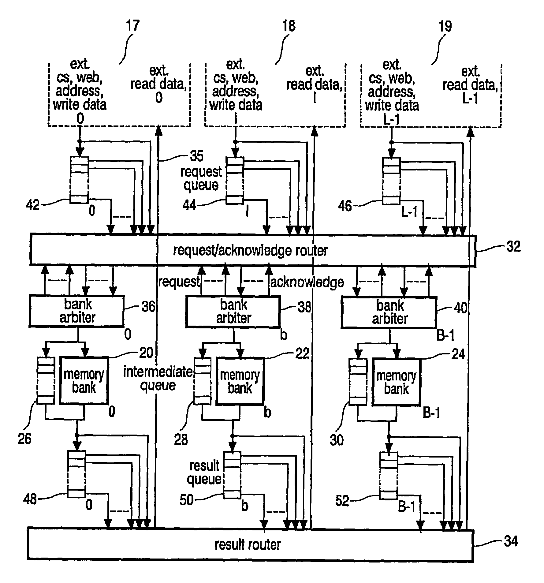
[0023]FIG. 1 illustrates a pseudo multiport data memory template or parametrizable embodiment. The template consists of an exemplary number of L building blocks (only the numbers 0, 1 , L−1 having been shown) that surround an array of B memory banks 20–24 (only the numbers 0 , b, and B−1 having been shown), each provided with an intermediate queue 26–30 that has been put in parallel between the input and the output of the memory module in question. The memory banks represent a unified address map. Generally, the values relate according to B≧L, but this is no restriction and in principle, the value of B may be as low as 1.

[0024]The external access signals may as shown at the top of the Figure, emanate from respective load / store unit facilites 17–19. Each access signal comprises a chip select cs, a write enable web, and each will furthermore present an address and write data. These signals will be sent to request / acknowledge router 32. In general, each external access facility will al...


PUM


Abstract

A computer memory arrangement comprises a first plurality of input port facilities (17–19) that are collectively coupled through a first router facility (32) to selectively feed a second plurality of memory modules (20–24). It furthermore comprises an output port facility that is collectively fed by said second plurality of memory modules (20–24). In particular, the computer memory arrangement comprises a detection facility (36–40) conflicting accesses through more than one of the first plurality of input port facilities, and for thereupon allowing only a single one among said simultaneous and conflicting accesses whilst generating a stall signal for signalling a mandatory stall cycle to a request source that implies an access latency thereto. The computer memory furthermore comprises a programming facility for having the access latency be selectably programmable according to an actual processing application.

Description

BACKGROUND OF THE INVENTION[0001]The invention relates to a computer memory arrangement, comprising a first plurality of input ports that are collectively coupled through a first router facility to selectively feed a second plurality of memory modules. Present-day computing facilities such as Digital Signal Processors (DSP) require both a great processing power, and also much communication traffic between memory and processor(s). Furthermore, ideally, both of these two performance aspects associated to the number of memory modules and processors, respectively, should be scalable, and in particular, the number of parallel data moves should be allowed to exceed the value of 2.[0002]As long as a scale of 2 were sufficient, a possible solution would be to have two fully separate and fully functional memories, but then the selecting for a storage location between the two memories represents a complex task. Obviously, the problem will be aggravated for scale factors that are higher than 2...

Claims


Application Information

Patent Timeline
Patent Type & Authority Patents(United States)
IPC IPC(8): G06F13/00G06F12/00G06F12/06G06F13/16
CPCG06F13/161
Inventor LEIJTEN, JEROEN ANTON JOHAN
Owner INTEL CORP