

Voltage subtracting circuit carrying out voltage subtraction by converting input voltage into current, intensity detecting circuit, and semiconductor integrated circuit device using the same
a voltage subtraction and input voltage technology, applied in the field of voltage subtraction circuits, intensity detection circuits, semiconductor integrated circuit devices, etc., can solve problems such as difficult detection
- Summary
- Abstract
- Description
- Claims
- Application Information
AI Technical Summary
Benefits of technology
Problems solved by technology
Method used
Image


Examples
first embodiment
[0082]With reference to FIG. 1, description will be given of a voltage subtracting circuit according to the present invention.
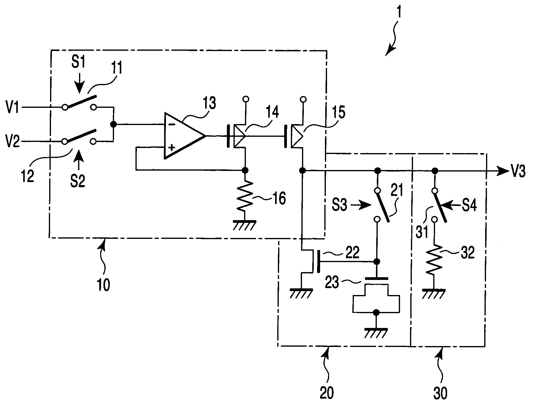
[0083]FIG. 1 is a circuit diagram of a voltage subtracting circuit according to a first embodiment of the present invention. As shown in the figure, the voltage subtracting circuit 1 comprises a voltage / current converting circuit 10, a voltage holding and current output circuit 20, and a voltage output section 30.
[0084]The voltage / current converting circuit 10 converts input voltages V1 and V2 into currents. The voltage / current converting circuit 10 comprises switch elements 11 and 12, an operational amplifier 13, a p-channel MOS transistors 14 and 15, and a resistance element 16. Control signals S1 and S2 control opening and closing of the switch elements 11 and 12. A voltage V1 is input to one end of the switch element 11. A voltage V2 is input to one end of the switch element 12. The other ends of the switch elements 11 and 12 are connected together and to...
fifth embodiment
[0126]Now, description will be given of a radio communication semiconductor integrated circuit comprising an intensity detecting circuit using the voltage subtracting circuit according to the present invention. The present embodiment relates to a technique for preventing the operational characteristics of the radio communication semiconductor integrated circuit from depending on the temperature by providing each circuit in the radio communication semiconductor integrated circuit with a current and voltage having a predetermined temperature characteristic (or having no temperature characteristic). FIG. 20 is a block diagram of the radio communication semiconductor integrated circuit according to the present embodiment, that is, a Bluetooth module.
fourth embodiment
[0127]As shown in the figure, the configuration of a Bluetooth module 80 corresponds to the configuration in FIG. 15 described in the fourth embodiment and to which a bias current / voltage generator 114 is added. Each circuit in the RF block 100 operates using a bias current and a bias voltage supplied by the bias current / voltage generator 114.
[0128]FIG. 21 is a block diagram of the bias current / voltage generator 114. As shown in the figure, the bias current / voltage generator 114 comprises a PTAT (Proportional To Absolute Temperature) bias generator 150, a reference voltage generator 151, an Iconst generator 152, an Iptat generator 153, an If generator 154, and a voltage / current generator 155.
[0129]The PTAT bias generator 150 generates a voltage Vp on the basis of an enable signal. The reference voltage generator 151 generates a predetermined reference voltage Vref2 on the basis of the voltage Vp generated by the PATA bias generator 150. The Iconst generator 152 generates a constant ...
PUM
 Abstract
Description
Claims
Application Information