
Methodology for recovery of hot carrier induced degradation in bipolar devices

a technology of hot carrier and bipolar transistor, which is applied in the field of bipolar transistors, can solve the problems of low avalanche hot carrier affecting the breakdown voltage of bipolar transistor, and reducing so as to increase the device performance, reduce the current gain of the device, and increase the base current

Inactive Publication Date: 2007-07-03
ULTRATECH INT INC
View PDF52 Cites 12 Cited by
  • Summary
  • Abstract
  • Description
  • Claims
  • Application Information

AI Technical Summary

Benefits of technology

"The present invention provides a method and structure for recovering avalanche degradation in bipolar transistors, especially SiGe HBTs, which is caused by avalanche hot carriers. The method involves subjecting the transistor to a thermal anneal step that increases the temperature of the transistor to recover the degradation. The thermal anneal can be performed using a self-heating structure or other annealing sources such as a furnace or laser. The recovered avalanche degradation is important for achieving high output power for radar and wireless communication applications. The structure of the invention includes a self-heating element that is present at the device level and can be used to increase the temperature of the bipolar transistor to recover avalanche degradation."

Problems solved by technology

The avalanche hot carriers create damage within the bipolar transistor and decrease the device's current gain by increasing base current.
Moreover, avalanche hot carriers affect the breakdown voltage of bipolar transistors, especially SiGe HBTs.
Specifically, a high avalanche current results in low breakdown voltage of the bipolar transistor.

Method used


Image

  • Methodology for recovery of hot carrier induced degradation in bipolar devices
  • Methodology for recovery of hot carrier induced degradation in bipolar devices
  • Methodology for recovery of hot carrier induced degradation in bipolar devices

Examples


Embodiment Construction

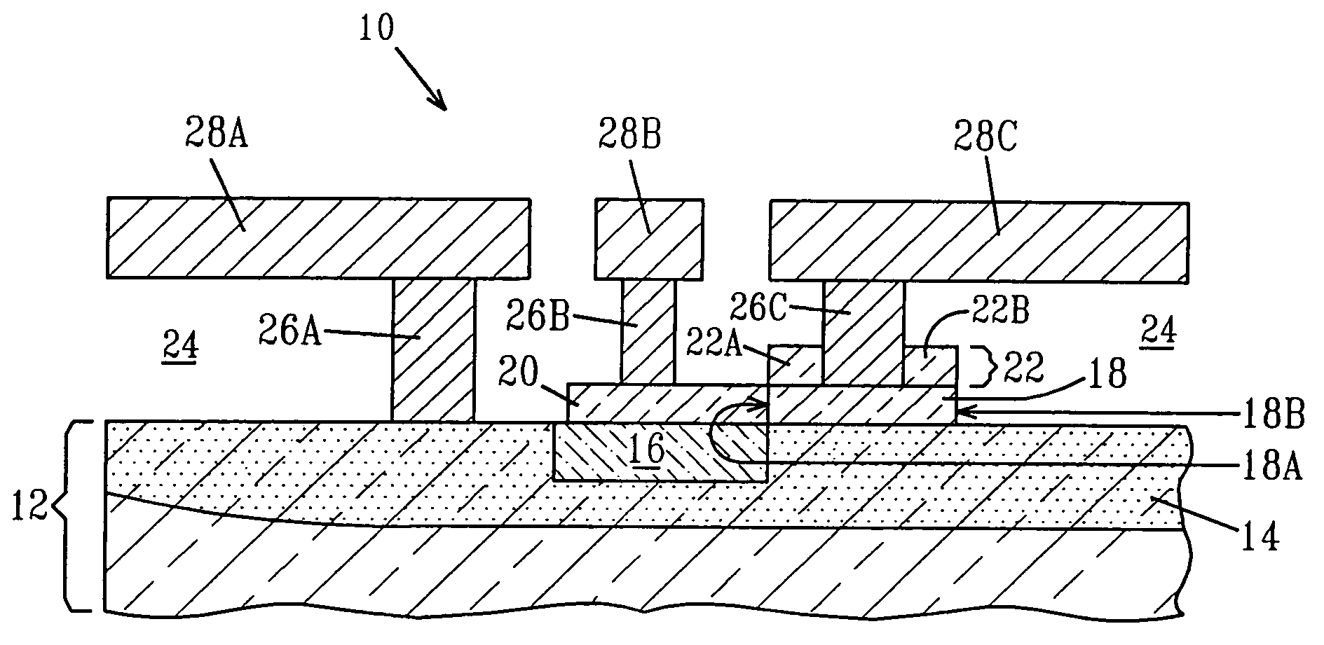
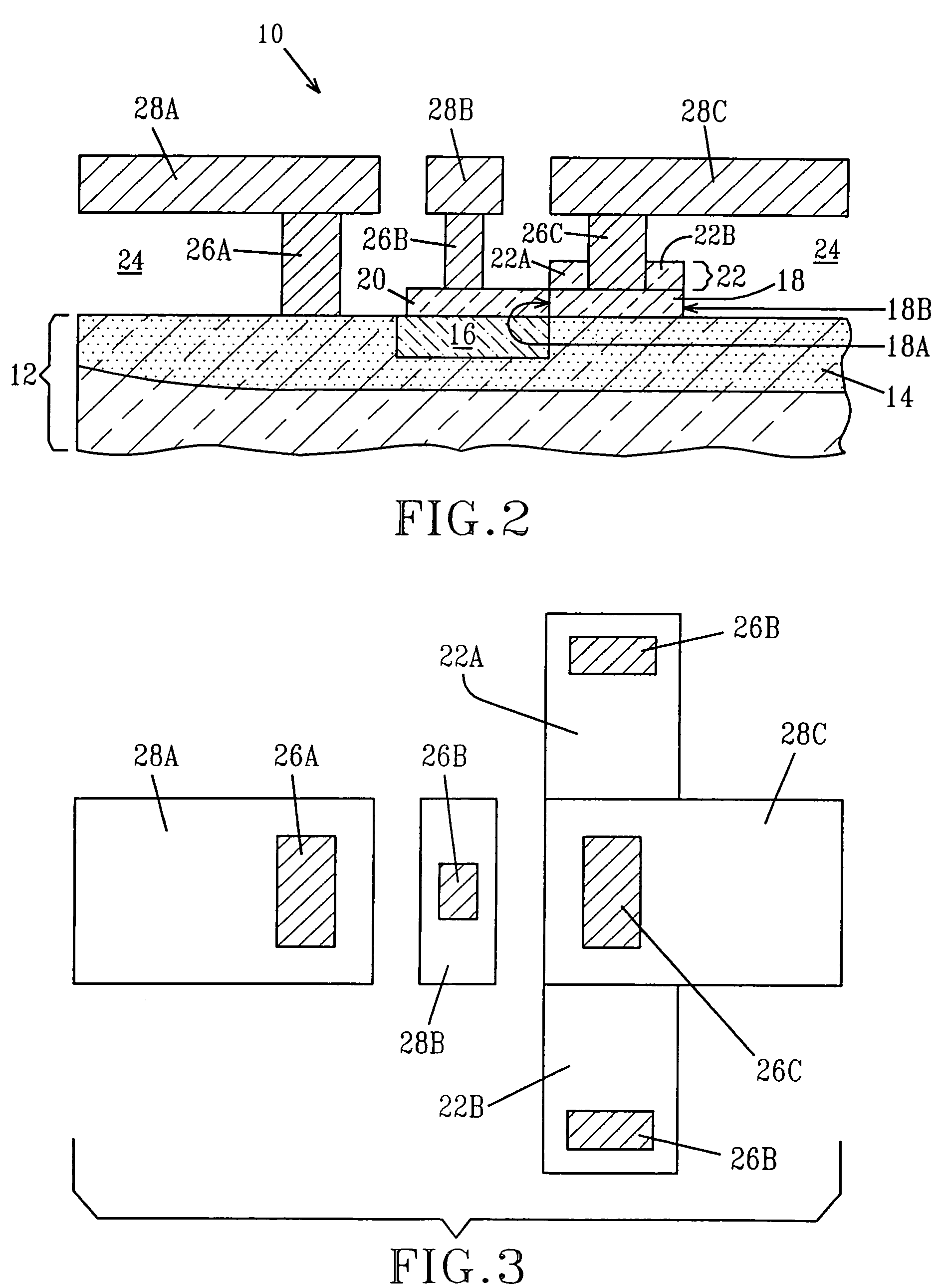
[0028]The present invention, which provides a method and structure that can be used for the recovery of device degradation cause by avalanche hot carriers, will now be described in more detail by referring to the following drawings that accompany the present application. It is noted that the drawings of the inventive structure are provided herein for illustrative purposes and thus they are not drawn to scale.

[0029]Reference is first made to FIG. 2 in which the inventive bipolar transistor structure including a self-heating element is shown. The term “bipolar transistor” includes any electronic device that includes two p-n junctions in close proximity to each other. The bipolar transistors include an emitter, a collector and a base positioned between the emitter and the collector. The present invention is specifically related to HBTs, and more particularly to SiGe HBTs. Specifically, FIG. 2 illustrates a bipolar transistor structure 10 that includes a Si-containing semiconductor subs...


PUM


Abstract

A method for recovery of degradation caused by avalanche hot carriers is provided that includes subjecting an idle bipolar transistor exhibiting avalanche degradation to a thermal anneal step which increases temperature of the transistor thereby recovering the avalanche degradation of the bipolar transistor. In one embodiment, the annealing source is a self-heating structure that is a Si-containing resistor that is located side by side with an emitter of the bipolar transistor. During the recovering step, the bipolar transistor including the self-heating structure is placed in the idle mode (i.e., without bias) and a current from a separate circuit is flown through the self-heating structure. In another embodiment of the present, the annealing step is a result of providing a high forward current (around the peak fT current or greater) to the bipolar transistor while operating below the avalanche condition (V″CB of less than 1 V). Under the above conditions, about 40% or greater of the degradation can be recovered. In yet another embodiment of the present invention, the thermal annealing step may include a rapid thermal anneal (RTA), a furnace anneal, a laser anneal or a spike anneal.

Description

FIELD OF THE INVENTION[0001]The present invention relates to bipolar transistors, and more particularly to silicon-containing, e.g., SiGe, heterojunction bipolar transistors (HBTs) that include a self-heating structure in the circuit level that obviates avalanche carrier related damages which typically decrease the drive current gain in both the forward and reverse bias mode. The present invention also provides a method for recovering hot carrier induced degradation of HBTs and other like bipolar transistors.BACKGROUND OF THE INVENTION[0002]Bipolar transistors are electronic devices with two p-n junctions that are in close proximity to each other. A typical bipolar transistor has three device regions: an emitter, a collector, and a base disposed between the emitter and the collector. Ideally, two p-n junctions, i.e., the emitter-base and collector-base junctions, are separated by a specific distance. Modulation of the current flow in one p-n junction by changing the bias of the near...

Claims


Application Information

Patent Timeline
Patent Type & Authority Patents(United States)
IPC IPC(8): H01L21/8249
CPCH01L29/7304H01L29/7378
Inventor GUARIN, FERNANDOHOSTETTER, JR., J. EDWINRAUCH, III, STEWART E.WANG, PING-CHUANYANG, ZHIJIAN J.
Owner ULTRATECH INT INC
Learn More