RF-MEMS switch and its fabrication method

a technology of micro-electromechanical systems and switches, applied in waveguide devices, relays, coatings, etc., can solve the problems of limited lowering voltage, warps that cannot be produced at room temperature, and are very difficult to suppress, so as to reduce the applied voltage, increase the coulomb force, and weaken the restoring force of the first spring

Inactive Publication Date: 2007-07-10
HITACHI MEDIA ELECTORONICS CO LTD
View PDF11 Cites 46 Cited by
  • Summary
  • Abstract
  • Description
  • Claims
  • Application Information

AI Technical Summary

Benefits of technology

[0011]A major object of the present invention is to solve these problems and provide a MEMS switch which operates at low voltage with stability and its fabrication method.
[0012]Further, an additional object of the present invention is to provide an inexpensive MEMS switch provided with a membrane which is of simple structure and attains high processing accuracy, and its fabrication method.
[0014]With the above structure, when voltage is applied to between the upper electrode and the lower electrode and the upper electrode gets close to the substrate, the Coulomb force is increased. In this stage, the second spring works and subsequently the upper electrode is brought into contact with the lower electrode. As the result, the switch is turned on. When voltage application is stopped and the switch is turned off, strong restoring force obtained by adding the restoring force of the first spring and that of the second spring is obtained. Thus, the upper electrode is separated from the lower electrode without fail. According to this, the restoring force of the first spring can be weakened, and the applied voltage can be lowered.
[0015]Further, to attain the above additional object, the following constitution is preferable: the first spring, first anchor, second spring, second anchor, and upper electrode are formed in integral structure to obtain a membrane. Further, these elements are preferably formed of a continuous identical metallic body. Thus, the membrane of integral structure is obtained by forming a metallic film once and patterning it. As a result, an inexpensive MEMS switch provided with a membrane which is of simple structure and attains high processing accuracy and its fabrication method are obtained.

Problems solved by technology

This brings a limitation to lowering voltage.
When a multilayer film is used, a warp may not be produced at room temperature.
For this reason, in a MEMS switch using a multilayer film, a warp is very difficult to suppress, and the temperature range within which low-voltage operation is feasible is inevitably and significantly narrowed.

Method used


Image

  • RF-MEMS switch and its fabrication method
  • RF-MEMS switch and its fabrication method
  • RF-MEMS switch and its fabrication method

Examples


first embodiment

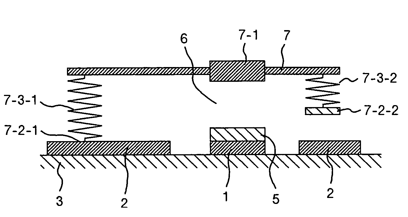
[0017]FIG. 1 is a schematic diagram explaining the MEMS switch according to the present invention.

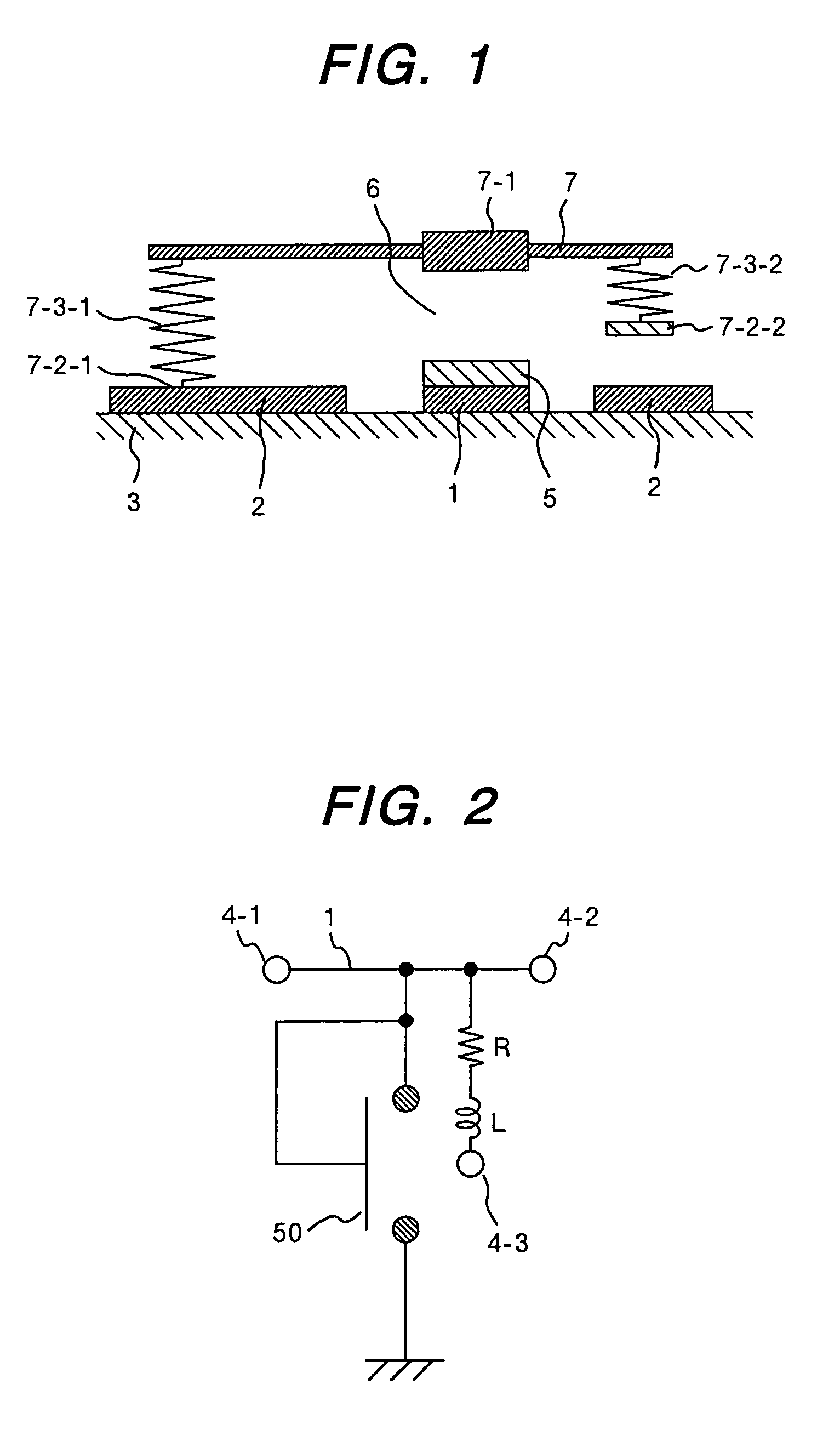
[0018]FIG. 2 is an equivalent circuit diagram explaining the first embodiment of the present invention and its control circuit.

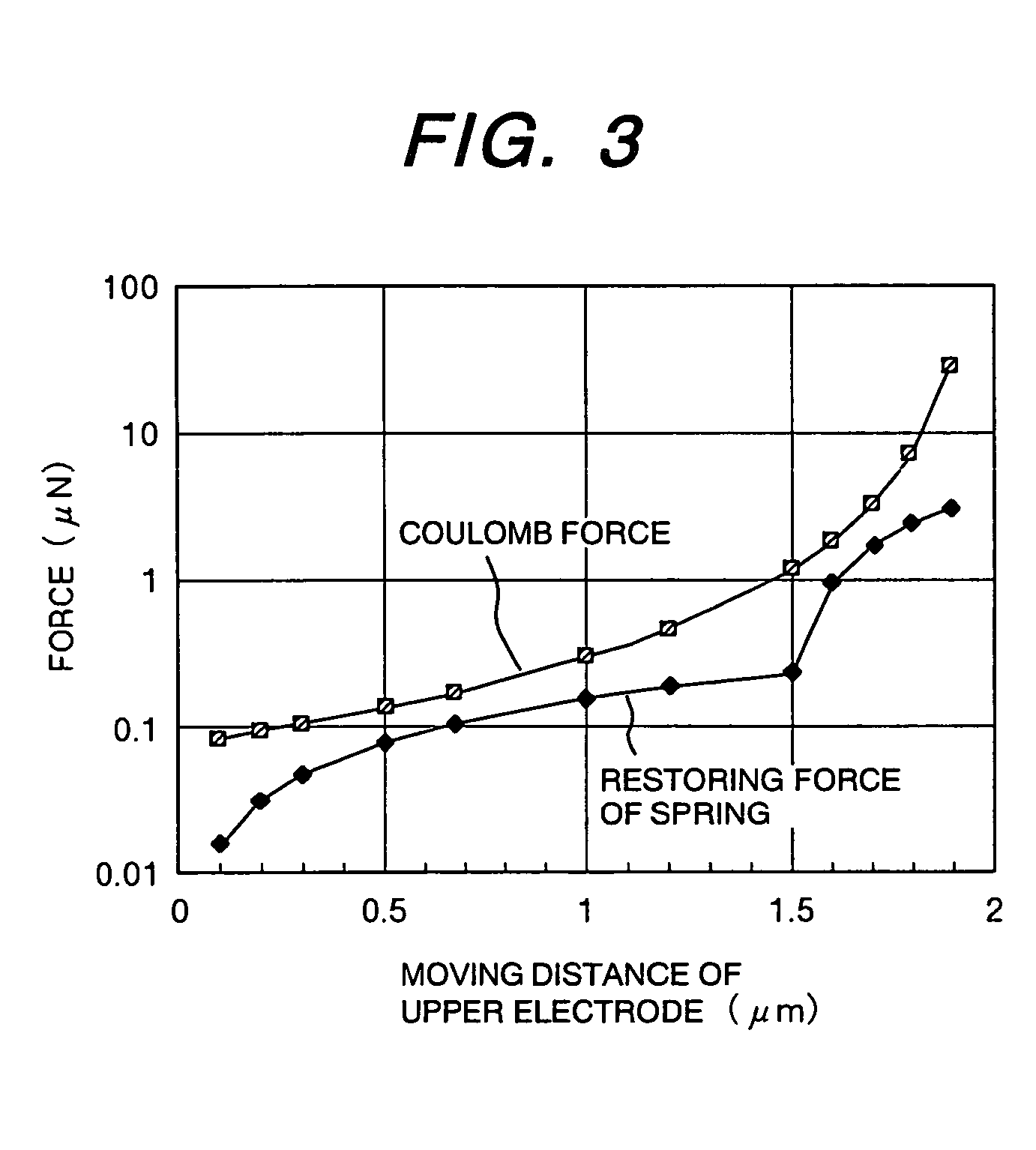
[0019]FIG. 3 is a curve chart illustrating the moving distance dependence of force exerted on the upper electrode in the first embodiment of the present invention.

second embodiment

[0020]FIG. 4 is a cross-sectional view explaining the present invention.

[0021]FIG. 5 is a top view explaining the second embodiment of the present invention.

[0022]FIG. 6 is a perspective view explaining the structure of the membrane in the second embodiment of the present invention.

third embodiment

[0023]FIG. 7 is a cross-sectional view explaining the present invention.

[0024]FIG. 8 is a top view explaining the third embodiment of the present invention.

[0025]FIG. 9 is a perspective view explaining the structure of the membrane in the third embodiment of the present invention.


PUM

PropertyMeasurementUnit
lengthaaaaaaaaaa
lengthaaaaaaaaaa
lengthaaaaaaaaaa

Abstract

The MEMS switch comprises a first anchor formed over a substrate, a first spring connected to the first anchor, an upper electrode which is connected to the first spring and makes a motion above the substrate, elastically deforming the first spring, a lower electrode formed over the substrate, positioned under the upper electrode, a second spring connected to the upper electrode, and a second anchor connected to the second spring. When voltage is applied between the upper and lower electrodes and the upper electrode makes a downward motion, the second anchor is brought into contact with the substrate. As a result, the second spring is elastically deformed. When the upper electrode is subsequently brought into contact with the lower electrode, thereby the upper and lower electrodes are electrically connected. The first and second anchors, first and second springs, and upper electrode are formed of identical metal in integral structure.

Description

CLAIM OF PRIORITY[0001]The present application claims priority from Japanese application JP 2003-379390 filed on Nov. 10, 2003, the content of which is hereby incorporated by reference in this application.FIELD OF THE INVENTION[0002]The present invention relates to a MEMS (Micro-Electro-Mechanical Systems) switch and its fabrication method. More particularly, it relates to a MEMS switch which turns on and off electrical signals of a wide range of frequency ranging from several hundreds of megahertz to several gigahertz or more and its fabrication method.BACKGROUND OF THE INVENTION[0003]Conventionally, MEMS switch has been known as a microscopic electromechanical component for turning on and off electrical signals. For example, the MEMS switch disclosed in Japanese Patent Laid-Open No. H9-17300 is fabricated over a substrate by a fine structure fabrication technique for use in the fabrication of semiconductor devices. A projection, which functions as an anchor (support), of an insula...

Claims


Application Information

Patent Timeline
Patent Type & Authority Patents(United States)
IPC IPC(8): H01H51/22B81B3/00B81C1/00H01H1/20H01H59/00H01P1/12
CPCH01H59/0009H01P1/127H01H1/20
Inventor ISOBE, ATSUSHITERANO, AKIHISAASAI, KENGOUCHIYAMA, HIROYUKIMATSUMOTO, HISANORI
Owner HITACHI MEDIA ELECTORONICS CO LTD
Why Eureka
Try Eureka