Thin film transistor array panel

a transistor array and thin film technology, applied in semiconductor devices, identification means, instruments, etc., can solve the problems of reducing the aperture ratio, affecting the display quality, and affecting the image quality, so as to secure the aperture ratio and minimize light leakage

Inactive Publication Date: 2007-07-10
SAMSUNG DISPLAY CO LTD
View PDF13 Cites 2 Cited by
  • Summary
  • Abstract
  • Description
  • Claims
  • Application Information

AI Technical Summary

Benefits of technology

[0008]A motivation of the present invention is to provide a thin film transistor array panel for a liquid crystal display capable of securing aperture ratio as well as minimizing light leakage.

Problems solved by technology

However, there is a problem that undesired inversion of the arrangement of the liquid crystal molecules occurs around contact holes of an insulating layer for connecting the pixel electrodes and the data wire, and this causes light leakage to show disclination, thereby degrading display quality.
Although the light leakage is blocked by designing opaque films such as the gate wire and the data wire to be wide, this reduces the aperture ratio, particularly for a high-resolution LCD.

Method used


Image

  • Thin film transistor array panel
  • Thin film transistor array panel
  • Thin film transistor array panel

Examples


first embodiment

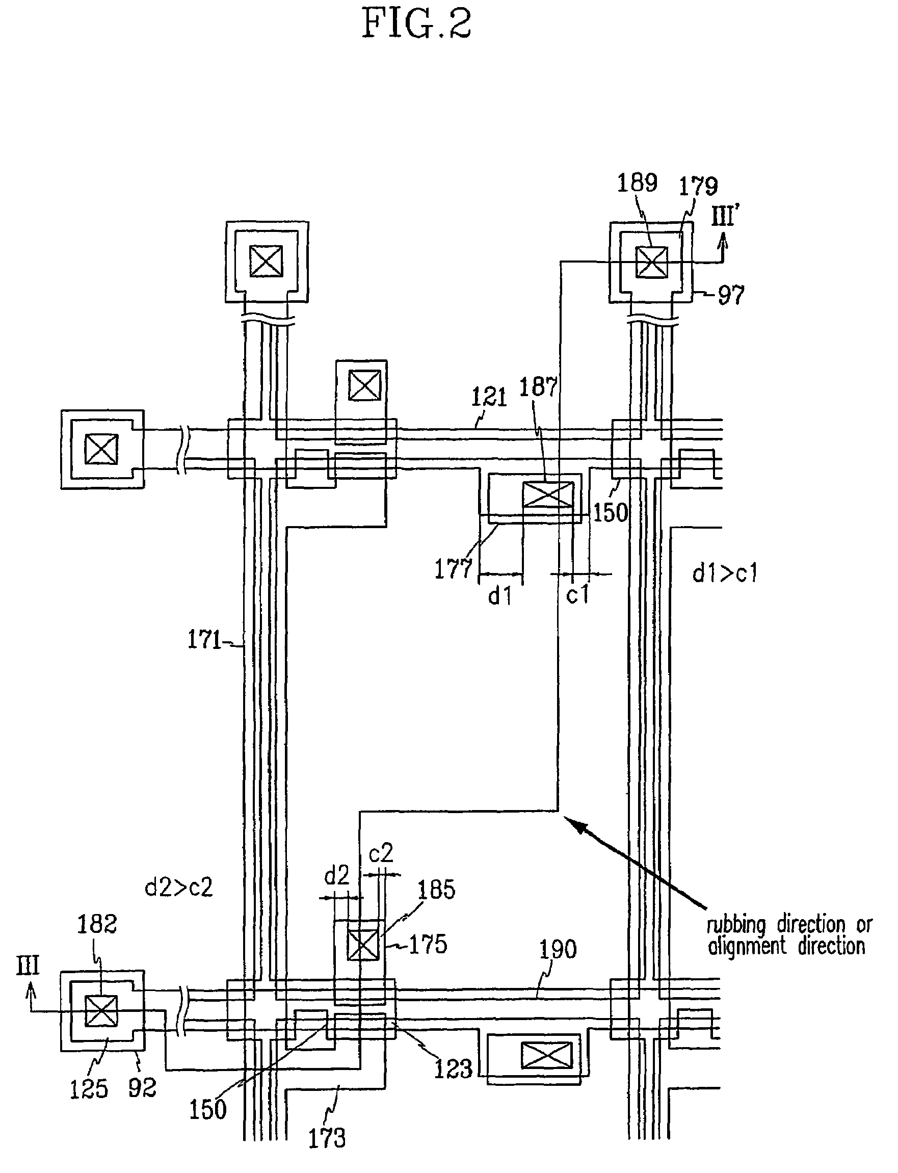
[0048]First, a TFT array panel for an LCD according to the present invention will be described in detail with reference to FIGS. 2 and 3.

[0049]FIG. 2 is a layout view of a TFT array panel for an LCD according to a first embodiment of the present invention, and FIG. 3 is a sectional view of the TFT array panel shown in FIG. 2 taken along the line III–III′.

[0050]A gate wire preferably made of a single layer made of Ag, Ag alloy, Al or Al alloy having low resistivity, or multi-layers including the single layer is formed on an insulating substrate 110. The gate wire includes a plurality of gate lines 121 extending in a transverse direction, a plurality of gate pads 125 connected to one ends of the gate lines 121 and transmits gate signals from an external device to the gate lines 121, and a plurality of gate electrodes 123 of TFTs connected to the gate lines 121. The gate wire overlaps storage capacitor conductors 177 connected to pixel electrodes 82 to form storage capacitors for enhan...

second embodiment

[0065]First, a pixel unit of a TFT array panel for an LCD according to the present invention with reference to FIGS. 8–10.

[0066]FIG. 8 is a layout view of a TFT array panel for an LCD according to a second embodiment of the present invention, and FIGS. 9 and 10 are sectional views of the TFT array panel shown FIG. 7 taken along the line IX–IX′ and the line X–X′, respectively.

[0067]A gate wire is formed on an insulating substrate 110. The gate wire includes a single layer or multi layers made of conductive material having low resistivity such as Ag, Ag alloy, Al, Al alloy, Cr or Ta. The gate wire includes a plurality of gate lines 121, a plurality of gate pads 125, and a plurality of gate electrodes 123. A storage capacitor wire is also formed on the substrate 110. The storage capacitor wire includes a plurality of storage capacitor lines 131 parallel to the gate lines 121 and supplied with an external voltage such as a common voltage to be applied to a common electrode of an upper p...

third embodiment

[0102]FIG. 18 is a layout view of a TFT array panel for an LCD according to the present invention, and FIG. 19 is a sectional view of the TFT array panel shown in FIG. 18 taken along the line XIX–XIX′.

[0103]Most of the structure is substantially the same as that of the first embodiment.

[0104]However, a plurality of red, green and blue color filters of R, G and B extending in a longitudinal direction are formed in respective pixel areas under a passivation layer 180. The color filters R, G and B have a plurality of apertures C1 and C2 exposing a plurality of drain electrodes 173 and a plurality of storage capacitor conductors 177, respectively. In this embodiment, the boundaries of the color filters R, G and B are shown to coincide with each other and to be located on a plurality of data lines 171. However, the color filters R, G and B may overlap each other on the data lines 171 to block the light leakage between the pixel areas. The color filters R, G and B are not formed near pad ...


PUM

PropertyMeasurementUnit
thicknessaaaaaaaaaa
conductiveaaaaaaaaaa
distanceaaaaaaaaaa

Abstract

A thin film transistor array panel according to the present invention includes a first wire, a second wire, and a pixel electrode. The first wire is formed on an insulating substrate and is used as a gate line or a storage capacitor electrode. The second wire overlaps the first wire via a gate insulating layer and is used as a storage capacitor conductor or a drain electrode. The pixel electrode is formed on a passivation layer covering the second wire and is connected to the second wire through a contact hole of a second insulating layer. In order to secure aperture ratio of the pixel and to block light leakage, distances between the boundaries of the contact hole at the place where alignment treatment or rubbing ends and the boundaries of the first wire or the second wire adjacent thereto and located outside the boundaries of the contact hole are designed to be wider than those between the boundaries of the contact hole at the other places and the boundaries of the first wire or the second wire.

Description

BACKGROUND OF THE INVENTION[0001](a) Field of the Invention[0002]The present invention relates to a thin film transistor array panel, and in particular, to a thin film transistor array panel used as a panel for a liquid crystal display.[0003](b) Description of the Related Art[0004]A typical liquid crystal display (“LCD”), which is one of widely used flat panel displays, includes two panels having a plurality of electrodes generating electric field, a liquid crystal layer interposed therebetween, and two polarizers attached to outer surfaces of the panels for polarizing light The LCD applies voltages to the electrodes to reorient liquid crystal molecules in the liquid crystal layer, thereby adjusting the amount of light passing therethrough. The LCD uses one of the characteristics that voltage application varies orientations of the liquid crystal molecules, and the LCD employing transmittance or reflection of light requires an internal or external light source since the liquid crysta...

Claims


Application Information

Patent Timeline
Patent Type & Authority Patents(United States)
IPC IPC(8): G02F1/1343G02F1/1368G02F1/133G02F1/1337G02F1/136G02F1/1362G09F9/30G09F9/35H01L29/786
CPCG02F1/133784G02F1/136209G02F1/136227G02F1/136213H01L27/1288G02F2001/13373G02F2001/136222G02F2201/40G02F1/136286G02F1/13373G02F1/136222G02F1/136
Inventor KIM, DONG-GYU
Owner SAMSUNG DISPLAY CO LTD
Why Eureka
Try Eureka