Printed circuit board for high speed, high density electrical connector with improved cross-talk minimization, attenuation and impedance mismatch characteristics

a high-density, electrical connector technology, applied in the direction of insulated conductors, coupling device connections, cables, etc., can solve the problems of reducing the use of single-ended signals in the system, reducing the possibility of electrical noise generated in the connector, and presenting a significant limitation on single-ended signal us

Active Publication Date: 2007-07-10
AMPHENOL CORP
View PDF15 Cites 18 Cited by
  • Summary
  • Abstract
  • Description
  • Claims
  • Application Information

AI Technical Summary

Problems solved by technology

Electronic systems have generally become smaller, faster and functionally more complex.
As signal frequencies increase, there is a greater possibility of electrical noise being generated in the connector in forms such as reflections, cross-talk and electromagnetic radiation.
It has thus been recognized that this presents a significant limitation on single-ended signal use for systems with growing numbers of higher frequency signal paths.
While the electrical connector disclosed in the '827 patent and other presently available differential

Method used


Image

  • Printed circuit board for high speed, high density electrical connector with improved cross-talk minimization, attenuation and impedance mismatch characteristics
  • Printed circuit board for high speed, high density electrical connector with improved cross-talk minimization, attenuation and impedance mismatch characteristics
  • Printed circuit board for high speed, high density electrical connector with improved cross-talk minimization, attenuation and impedance mismatch characteristics

Examples


Embodiment Construction

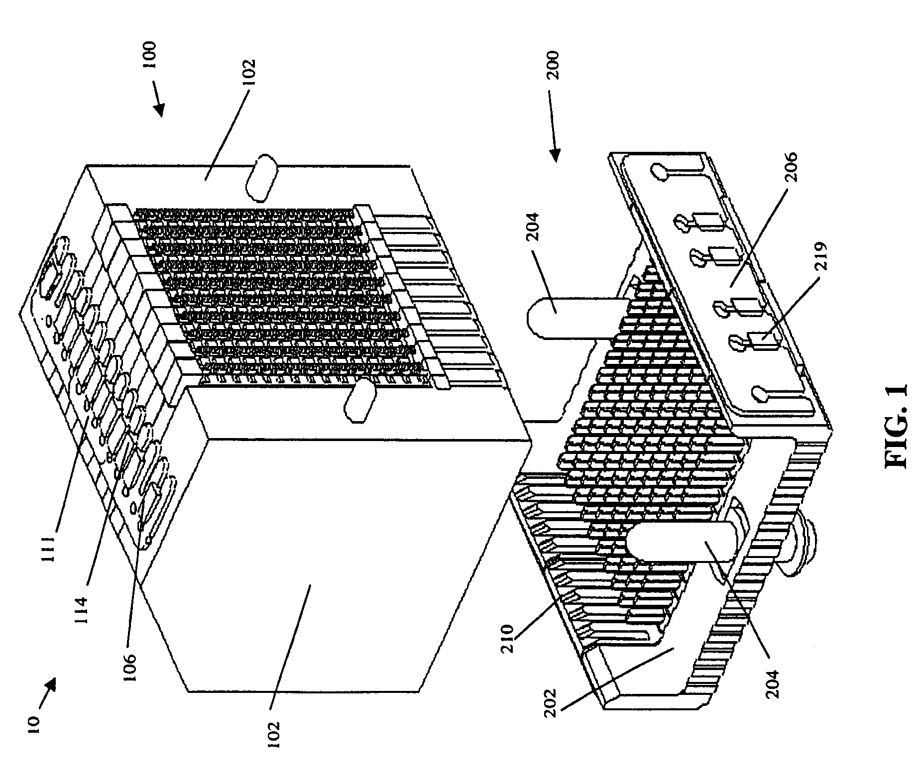
[0035]Referring to FIG. 1, there is shown an electrical connector assembly in accordance with an embodiment of the present invention. The electrical connector assembly 10 includes a first electrical connector 100 mateable to a second electrical connector 200.

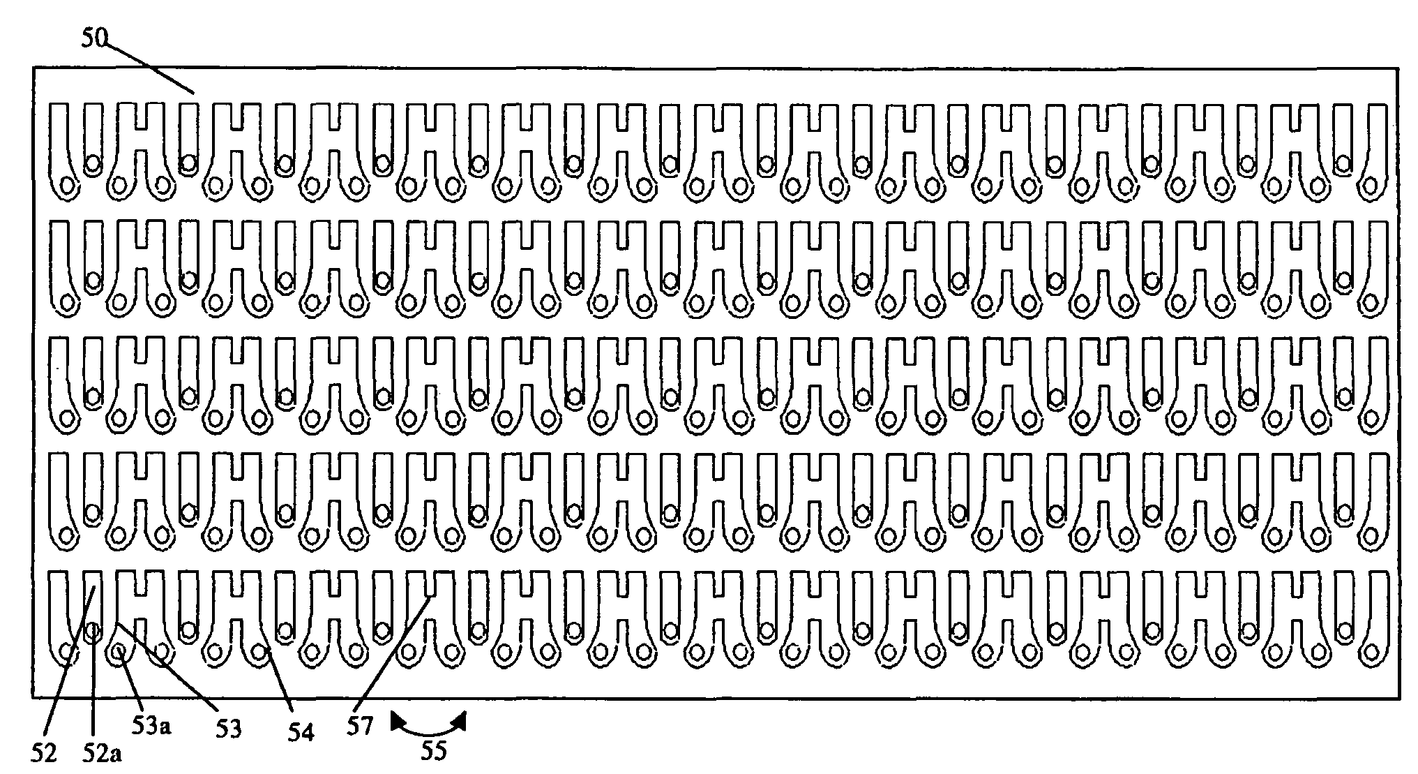
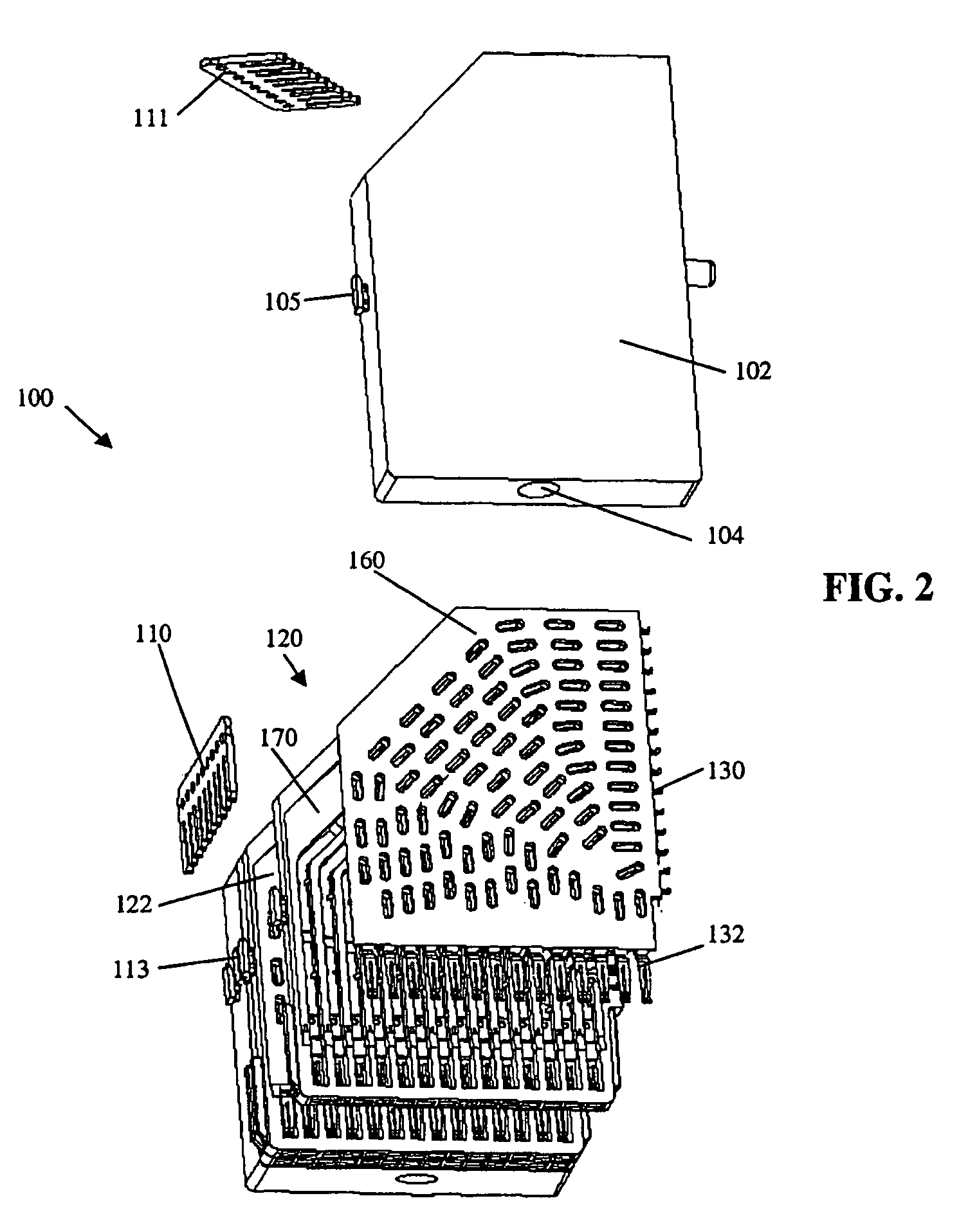
[0036]The first electrical connector 100, which is shown in greater detail in FIGS. 2–8b, includes a plurality of wafers 120, with each of the plurality of wafers 120 having an insulative housing 122, a plurality of signal conductors 124 (see FIG. 3) and a plurality of shield strips 126 (see FIGS. 5a and 5b). For exemplary purposes only, the first electrical connector 100 is illustrated with ten wafers 120, with each wafer 120 having fourteen single-ended signal conductors 124 and corresponding fourteen shield strips 126. However, as it will become apparent later, the number of wafers and the number of signal conductors and shield strips in each wafer may be varied as desired.

[0037]The first electrical connector 100 is also show...


PUM


Abstract

In the preferred embodiment, there is disclosed a printed circuit board having a surface providing a mating interface to which is electrically connected an electrical connector having signal conductors and ground conductors. The printed circuit board includes a plurality of stacked dielectric layers, with a conductor disposed on at least one of the plurality of dielectric layers. The mating interface includes a plurality of conductive vias aligned in a plurality of rows, with the plurality of conductive vias extending through at least a portion of the plurality of dielectric layers, at least one of the plurality of conductive vias intersecting the conductor. The plurality of conductive vias includes signal conductor connecting conductive vias and ground conductor connecting conductive vias. For each of the plurality of rows of the conductive vias, there are at least twice as many ground conductor connecting conductive vias as signal conductor connecting conductive vias and the conductive vias are positioned relative to one another so that for each signal conductor connecting conductive via, there are ground conductor connecting conductive vias adjacent either side of the signal conductor connecting conductive via.

Description

BACKGROUND OF THE INVENTION[0001]This invention relates generally to an electrical connector assembly for interconnecting printed circuit boards. More specifically, this invention relates to a high speed, high density electrical connector assembly that provides improved cross-talk minimization and improved attenuation and impedance mismatch characteristics.[0002]Electrical connectors are used in many electronic systems. It is generally easier and more cost effective to manufacture a system on several printed circuit boards (“PCBs”) which are then connected to one another by electrical connectors. A traditional arrangement for connecting several PCBs is to have one PCB serve as a backplane. Other PCBs, which are called daughter boards or daughter cards, are then connected through the backplane by electrical connectors.[0003]Electronic systems have generally become smaller, faster and functionally more complex. This typically means that the number of circuits in a given area of an ele...

Claims


Application Information

Patent Timeline
IPC IPC(8): H05K1/11H01R12/16H05K1/02H05K3/42
CPCH01R13/65807H05K1/0219H01R13/6587H01R12/714H01R13/6471H01R13/6477H01R13/514H05K1/112H05K3/429H05K2201/09381H05K2201/09709H05K2201/10189H05K2201/09627
Inventor PAYNE, JASON J.GAILUS, MARK W.KHILCHENKO, LEON M.REN, HUILIN
Owner AMPHENOL CORP
Why Eureka
Try Eureka