Method for forming a buried diffusion layer with reducing topography in a surface of a semiconductor substrate

a technology of buried diffusion layer and semiconductor substrate, which is applied in the direction of semiconductor devices, electrical equipment, basic electric elements, etc., can solve the problems of difficult formation of salicide on the sidewall of shallow, and achieve the effect of reducing the resistance of the buried diffusion layer and improving the formation of a buried diffusion layer

Active Publication Date: 2007-07-17
MACRONIX INT CO LTD
View PDF1 Cites 0 Cited by
  • Summary
  • Abstract
  • Description
  • Claims
  • Application Information

AI Technical Summary

Benefits of technology

[0008]It is one objective of the present invention to provide a method for forming a buried diffusion layer with reducing topography in a surface of a semiconductor substrate, which utilizes a field oxide process to reduce topography of trenches following formed in a surface of the semiconductor substrate, thereby improving formation of a buried diffusion layer along the trenches in the semiconductor substrate.
[0009]It is another objective of the present invention to provide a method for forming a buried diffusion layer with reducing topography in a surface of a semiconductor substrate, which provides a buried diffusion layer with uniform distribution of dopants and let a salicide easily formed on the buried diffusion layer.
[0011]The present invention provides a plurality of shallow trenches on the surface of the semiconductor substrate, which improves formation of a buried diffusion layer along the surroundings of the shallow trenches by ion implantation. A salicide is also easily formed on the sidewall of the shallow trenches adjacent to the buried diffusion layer to reduce resistance of the buried diffusion layer.

Problems solved by technology

And, it is difficult to form the salicide on the sidewall of the shallow trench 16a due to poor step coverage.

Method used


Image

  • Method for forming a buried diffusion layer with reducing topography in a surface of a semiconductor substrate
  • Method for forming a buried diffusion layer with reducing topography in a surface of a semiconductor substrate
  • Method for forming a buried diffusion layer with reducing topography in a surface of a semiconductor substrate

Examples


Embodiment Construction

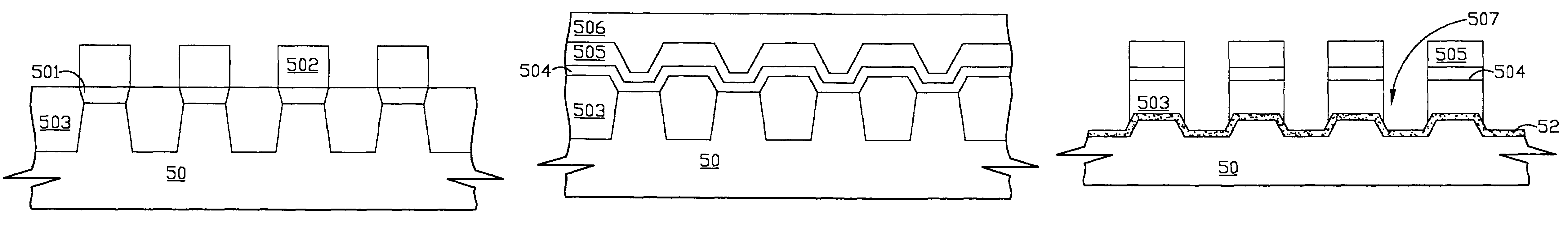
[0021]The present invention provides a field oxide process to reduce topography of shallow trenches following formed in a surface of a semiconductor substrate, thereby improving formation of a buried diffusion layer along the shallow trenches in the semiconductor substrate. A salicide is also easily formed along the sidewall of the shallow trenches adjacent to the buried diffusion layer.

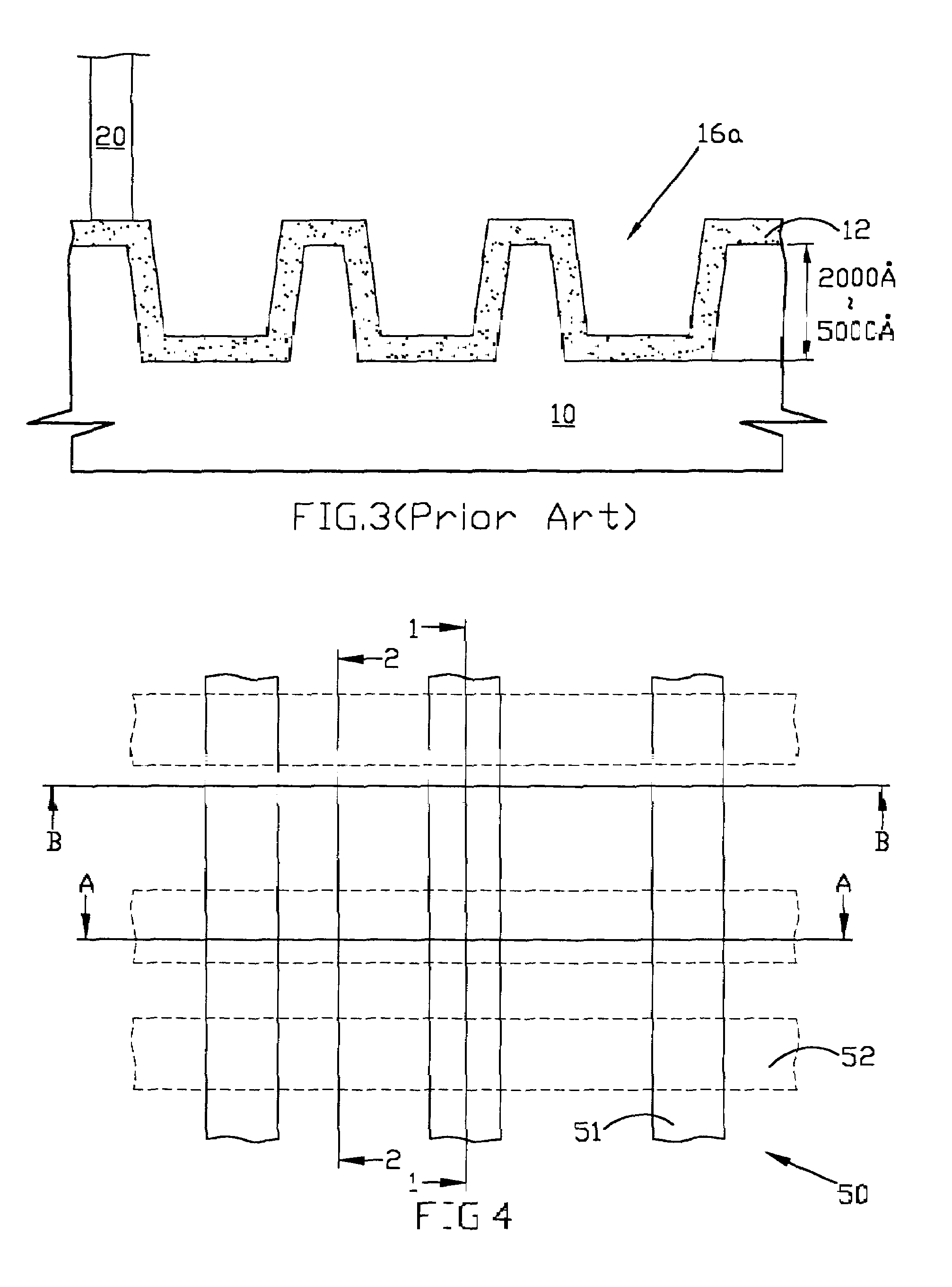
[0022]The present method will be described in detail according to one preferred embodiment of the present invention. FIG. 5A to FIG. 9B is schematic cross-sectional views of various steps of the preferred embodiment. FIG. 4 is a schematic top view of a structure provided by the preferred embodiment, in which a plurality of shallow trench isolation regions 51 is formed on the surface of a semiconductor substrate 50, and a plurality of buried diffusion layers 52 is formed in the surface of the semiconductor substrate 50 surrounding the shallow trench isolation regions 51. FIGS. 5A, 6A, 7A, 8A and 9A ar...


PUM

PropertyMeasurementUnit
depthaaaaaaaaaa
temperatureaaaaaaaaaa
conductivity typeaaaaaaaaaa

Abstract

A method for forming a buried diffusion layer with reducing topography in a surface of a semiconductor substrate is provided. A patterned first dielectric layer is formed on a semiconductor substrate for being used as a first hard mask. A thermal oxidation process is performed to form field oxides on the exposed potions of the semiconductor substrate. The patterned first dielectric layer is then removed. A second patterned dielectric layer is formed on the field oxides and the semiconductor substrate for being used as a second hard mask. An isotropic etching process is performed to etch the exposed portions of the field oxides and the semiconductor substrate. The patterned second dielectric layer and the underlying field oxides are removed to form a plurality of trenches on the surface of the semiconductor substrate. A buried diffusion layer is formed along surroundings of the trenches in the semiconductor substrate.

Description

BACKGROUND OF THE INVENTION[0001]1. Field of the Invention[0002]The present invention relates to a method for forming a buried diffusion layer in a surface of a semiconductor substrate, and more particularly to a method for forming a buried diffusion layer having reducing topography in a semiconductor substrate.[0003]2. Description of the Prior Art[0004]To satisfy the demands for high integration, low cost and high-speed operation, both of a buried diffusion layer and a salicidation technology are utilized for fabricating semiconductor devices. For example, FIG. 1 is a top view of a conventional flash memory device, which is provided with buried diffusion layers and shallow trench isolation regions. A buried diffusion layer 12 is formed in a surface of a semiconductor substrate 10 to serve as source and drain regions of memory cells. A word line 14 is formed on the semiconductor substrate 10 adjacent to one side of the buried diffusion layer 12. And, a plurality of shallow trench is...

Claims


Application Information

Patent Timeline
Patent Type & Authority Patents(United States)
IPC IPC(8): H01L21/76
CPCH01L27/115H01L27/11521H10B69/00H10B41/30
Inventor YIH, CHENG-MINGCHEN, HUEI-HUARNGKAO, HSUAN-LING
Owner MACRONIX INT CO LTD
Why Eureka
Try Eureka