Memory cell structure with capacitor over transistor

a memory cell and capacitor technology, applied in the direction of transistors, electrical devices, semiconductor devices, etc., can solve the problems of the capacitor, the structure of the 1t1c memory cell is very difficult to be further scaled down, and the leakage current of the storage capacitor is significantly reduced, so as to achieve the effect of reducing leakage current, reducing leakage current, and maintaining the capacitance of the storage capacitor at a reasonable scal

Pending Publication Date: 2021-11-18
ETRON TECH INC +1
View PDF4 Cites 4 Cited by
  • Summary
  • Abstract
  • Description
  • Claims
  • Application Information

AI Technical Summary

Benefits of technology

[0006]The present invention provides a new memory cell structure applied to DRAM, wherein the memory cell structure vertically integrates a storage capacitor (1C) directly over an access transistor (1T). The memory cell structure utilizing a 3D (three-dimensional) elevated source electrode with well-designed graded doping concentration with self alignment to a gate structure of the access transistor can significantly reduce leakage currents down to a range of femto-Amperes, wherein the leakage currents include the most difficult leakage source such as GIDL (Gate Induced Drain Leakage) and the junction leakages. Since the leakage currents are significantly reduced, capacitance of the storage capacitor can be maintained at a reasonable scale as the technology must be scaled down for reducing parasitic capacitance of the memory cell structure. The 3D elevated source electrode is also extended by a self-alignment technology to be connected to the signal storage node of the storage capacitor. Since the 1C is further being formed in a self-alignment way directly over the access transistor like an electric Tower over a residence, the memory cell structure is named as Tower capacitor over access Transistor, ToT Cell. Moreover, the present invention also provides a new Counter-electrode Plate of the storage capacitor, wherein the Counter-electrode Plate uses a metal material to cover over a high-K-dielectric-Insulator almost down to a surface of an active region of the access transistor and up to a top surface of the storage capacitor as a very solid (i.e. extremely low impedance and low noise) Constant-voltage Plane (usually biased at Half-VCC voltage level) for the storage capacitor. An underground bit line of the memory cell structure is used to reduce topography of the memory cell structure and self aligned to be connected to the drain region of the access transistor, those giving a well-designed orthogonal structure to the word line with much reduced coupling effect between the underground bit line and the word line. In addition, both parasitic capacitance and resistor-capacitor (RC) time constant in association with the underground bit line are reduced to allow more bits to be connected to the underground bit line or to enlarge the sensing signal which is a ratio of the capacitance of the storage capacitor to the bit line capacitance. The vertically constructed Counter-electrode Plate can also create a flat surface of the ToT Cell covered well by the metal material. This should give a better distribution of the electric fields inside the memory cell structure and a better thermal dissipation effect. The structure of the word line which is different from the state-of-the-art buried word-line structure has its invention to be self-aligned to the gate structure of the access transistor. Since most of the word line, the underground bit line, the source region, and the drain regions, the signal electrode, the counter-electrode plate, and all their related connections are formed by self-alignment processing techniques, the ToT Cell size is more controllable as the technology is scaled, which gives the solution of extending the 1T1C memory cell to be scaled down below 10 nanometers.

Problems solved by technology

The major problem is that a structure of the 1T1C memory cell is very hard to be further scaled down by even using very aggressive design rules which scales down the access transistor (i.e. 1T) and three-dimensional storage capacitor (i.e. 1C) such as a stacked capacitor over part of the access transistor and isolation areas or a very deep trench capacitor which may be positioned lower than the access transistor.
The difficulties for the 1T1C memory Cell are elaborated here though they are well-known problems even under huge financial, and research and development investments on technology, design and equipments.
To give a few examples of the difficulties: (1) the structure of the access transistor suffers unavoidable but more serious current leakage problem to degrade the 1T1C memory cell storage functions such as reducing the DRAM refresh time; (2) the complexities of arranging the word lines, bit lines and storage capacitors on their geometric and topographic structures and connections among the word lines, the bit lines, the storage capacitors, and the gates, sources and drains of the access transistors are getting much worse for scaling down; (3) the trench capacitor suffers too large aspect ratio of the depth versus opening size and is almost halted at the 14nm node; (4) the stacked capacitor suffers the worsen topography and there is almost no space for the contact spaces between the storage electrode to the source of the access transistor after twisting the active region from 20 degree to over 50 degree, etc.
In addition, the allowable space for the bit line contact to the drain of the access transistor is getting so small but a self-aligned feature must still be struggled to maintain; (5) the worsen leakage current problem demands enhancing the capacitance of the stacked capacitor and keeping increasing the height of the stacked capacitor to have a larger capacitance area unless a much high-K dielectric insulator material which is used for getting the higher storage capacitance can be discovered; (6) because all increasing demands on better reliability, quality and resilience of DRAM chips under increasingly demanding higher density / capacity and performance are getting harder to be met, and so on.
State-of-the-art has no technology breakthroughs of solving the above difficulties.
Therefore, how to design a new structure of the 1T1C memory cell to solve the above difficulties has become an important issue for a designer of the 1T1C memory cell.

Method used


Image

  • Memory cell structure with capacitor over transistor
  • Memory cell structure with capacitor over transistor
  • Memory cell structure with capacitor over transistor

Examples


Embodiment Construction

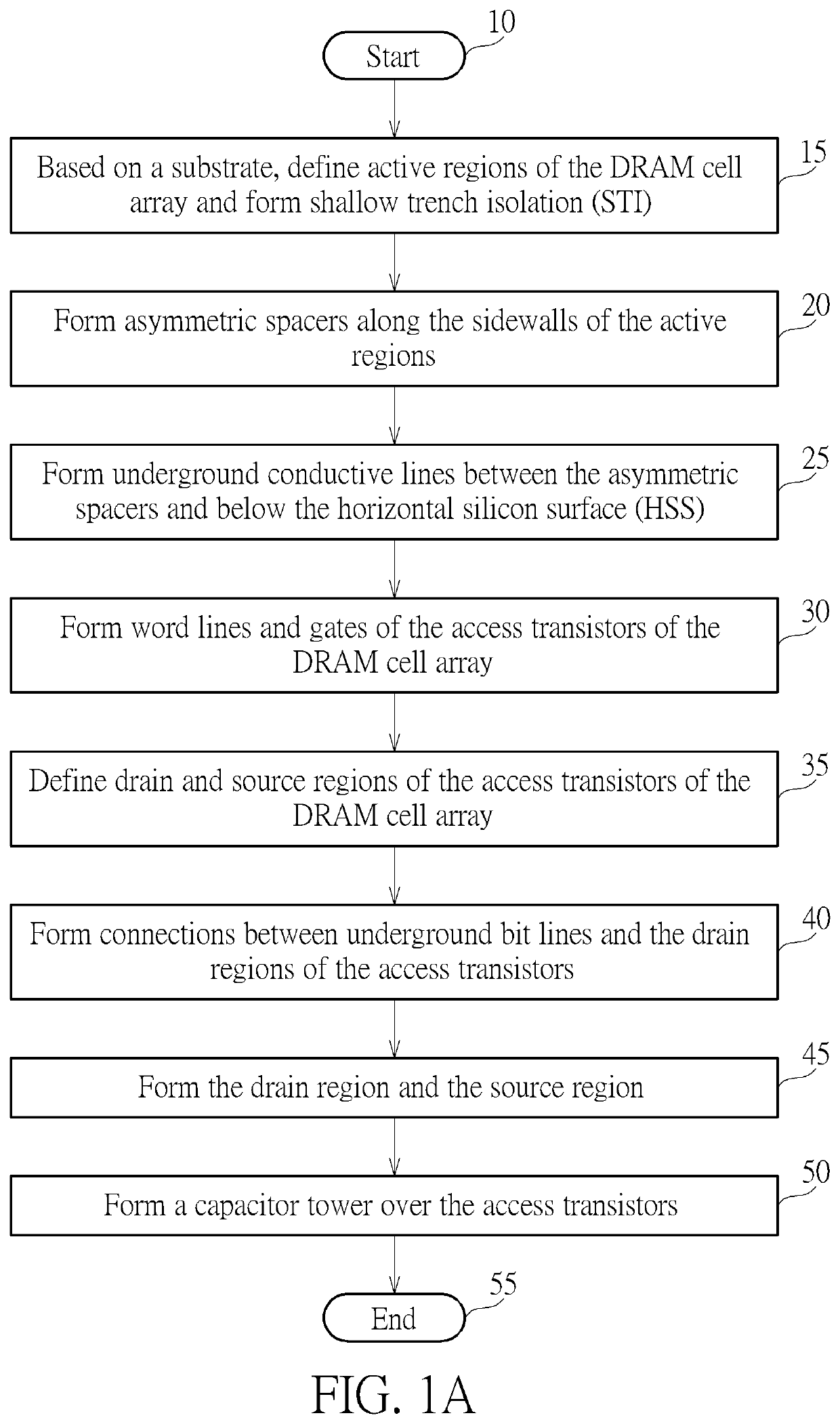
[0100]Please refer to FIGS. 1A-1F, wherein FIG. 1A is a flowchart illustrating a manufacturing method of a DRAM cell (1T1C cell) array according to an embodiment of the present invention.

[0101]Step 10: Start.

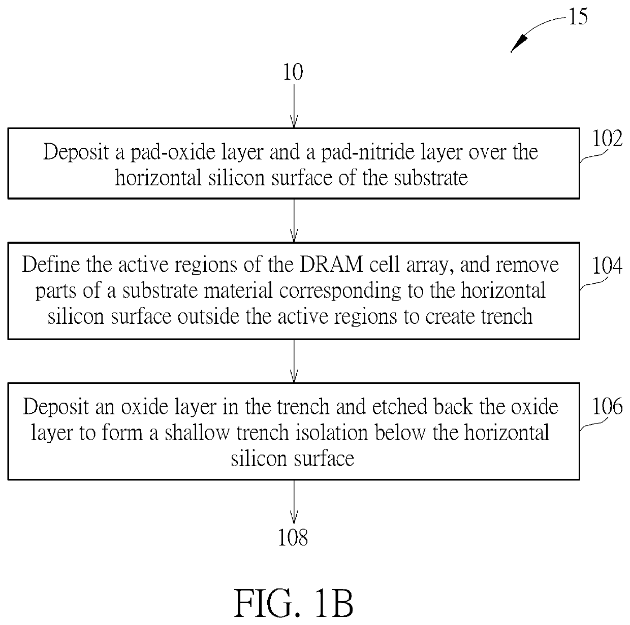
[0102]Step 15: based on a substrate (such as, a p-type silicon substrate), define active regions of the DRAM cell array and form shallow trench isolation (STI).

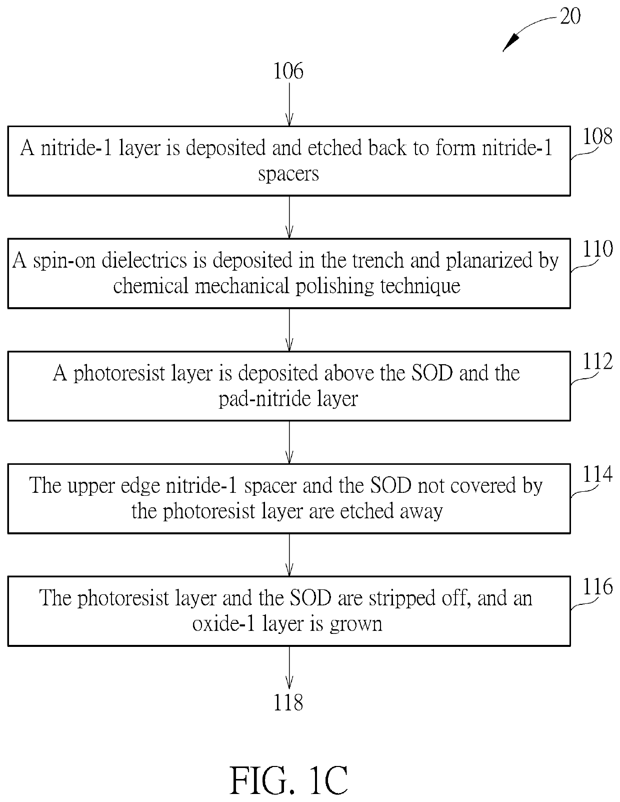
[0103]Step 20: Form asymmetric spacers along the sidewalls of the active regions.

[0104]Step 25: Form underground conductive lines (such as bit lines) between the asymmetric spacers and below the horizontal silicon surface (HSS).

[0105]Step 30: Form word lines and gates of the access transistors of the DRAM cell array.

[0106]Step 35: Define drain (i.e. first conductive regions) and source regions (i.e. second conductive regions) of the access transistors of the DRAM cell array.

[0107]Step 40: Form connections between underground bit lines and the drain regions of the access transistors.

[0108]Step 45: Form the drain region and...


PUM

PropertyMeasurementUnit
feature sizeaaaaaaaaaa
sizeaaaaaaaaaa

Abstract

A memory cell structure includes a silicon substrate, a transistor, a bit line, and a capacitor. The silicon substrate has a silicon surface. The transistor is coupled to the silicon surface, wherein the transistor includes a gate structure, a first conductive region, and a second conductive region. The bit line is electrically coupled to the first conductive region of the transistor and positioned under the silicon surface. The capacitor is over the transistor and electrically coupled to the second conductive region of the transistor.

Description

CROSS REFERENCE TO RELATED APPLICATIONS[0001]This application claims the benefit of U.S. Provisional Application No. 63 / 023,878, filed on May 13, 2020 and entitled “DRAM Cell of a Vertically Integrated 1C-over-1T Structure by Self-Alignment Processes”, the contents of which are incorporated herein by reference.BACKGROUND OF THE INVENTION1. Field of the Invention[0002]The present invention relates to a memory cell structure with capacitor over transistor, and particularly to a memory cell structure that has denser structure, smaller area, lower leakage currents, higher capacitance, and so on.2. Description of the Prior Art[0003]One of the most important volatile-memory integrated circuits is the DRAM (Dynamic Random Access Memory) using the 1T1C memory cell, which not only provides the best cost-performance function as main memory and / or buffer memory for computing and communication applications but also has acted as the best driver for technology scaling-down to sustain the Moore's ...

Claims


Application Information

Patent Timeline
Patent Type & Authority Applications(United States)
IPC IPC(8): H01L27/108
CPCH01L27/10832H10B12/30H10B12/315H10B12/05H10B12/033H10B12/0335H10B12/482H10B12/373
Inventor LU, CHAO-CHUN
Owner ETRON TECH INC
Why Eureka
Try Eureka