Integrated anneal cap/ ion implant mask/ trench isolation structure for III-V devices

a technology of ion implant mask and trench isolation structure, which is applied in the direction of semiconductor devices, basic electric elements, electrical apparatus, etc., can solve the problems of high device integration level, complex interconnection of these devices, and lack of capping layer, etc., to reduce device-level metal capacitance, reduce topography, and reduce the effect of device-level metal capacitan

Inactive Publication Date: 2005-09-22
JOHNSON DAVID ALAN +1
View PDF21 Cites 6 Cited by
  • Summary
  • Abstract
  • Description
  • Claims
  • Application Information

AI Technical Summary

Benefits of technology

[0018] The resulting structure is significantly more planar than the traditional composite dielectric structure used with III-V VLSI devices. This structure allows for reduced device-level metal capacitance, low active area to active area leakage, and topography reduction compared to conventional III-V bipolar structures. Finally, this structure is compatible with III-V semiconductors, and allows for use of a dry etch for removal of the final dielectric layer over the active semiconductor, where traditional silicon structures do not.

Problems solved by technology

The resulting isolation topography greatly complicates the interconnect of these devices.
High levels of device integration have not been achieved for III-V bipolar transistors with these isolation last process integration schemes.
Structures, often referred to as “shallow trench isolation” used in silicon processing to reduce topography rely on silicon specific etches, thermal oxidation to round the trench corners, and do not provide the necessary capping layer required by III-V semiconductors.
Such structures are also not compatible with III-V semiconductors, and they require the use of a wet etch to remove the final dielectric covering the active regions.
Wet etches have disadvantages such as high interfacial etch rates resulting in increased defect densities.
Groove isolation structures as disclosed in U.S. Pat. No. 5,293,061 do not provide the planarity necessary for defining subsequent fine geometries.

Method used


Image

  • Integrated anneal cap/ ion implant mask/ trench isolation structure for III-V devices
  • Integrated anneal cap/ ion implant mask/ trench isolation structure for III-V devices
  • Integrated anneal cap/ ion implant mask/ trench isolation structure for III-V devices

Examples


first embodiment

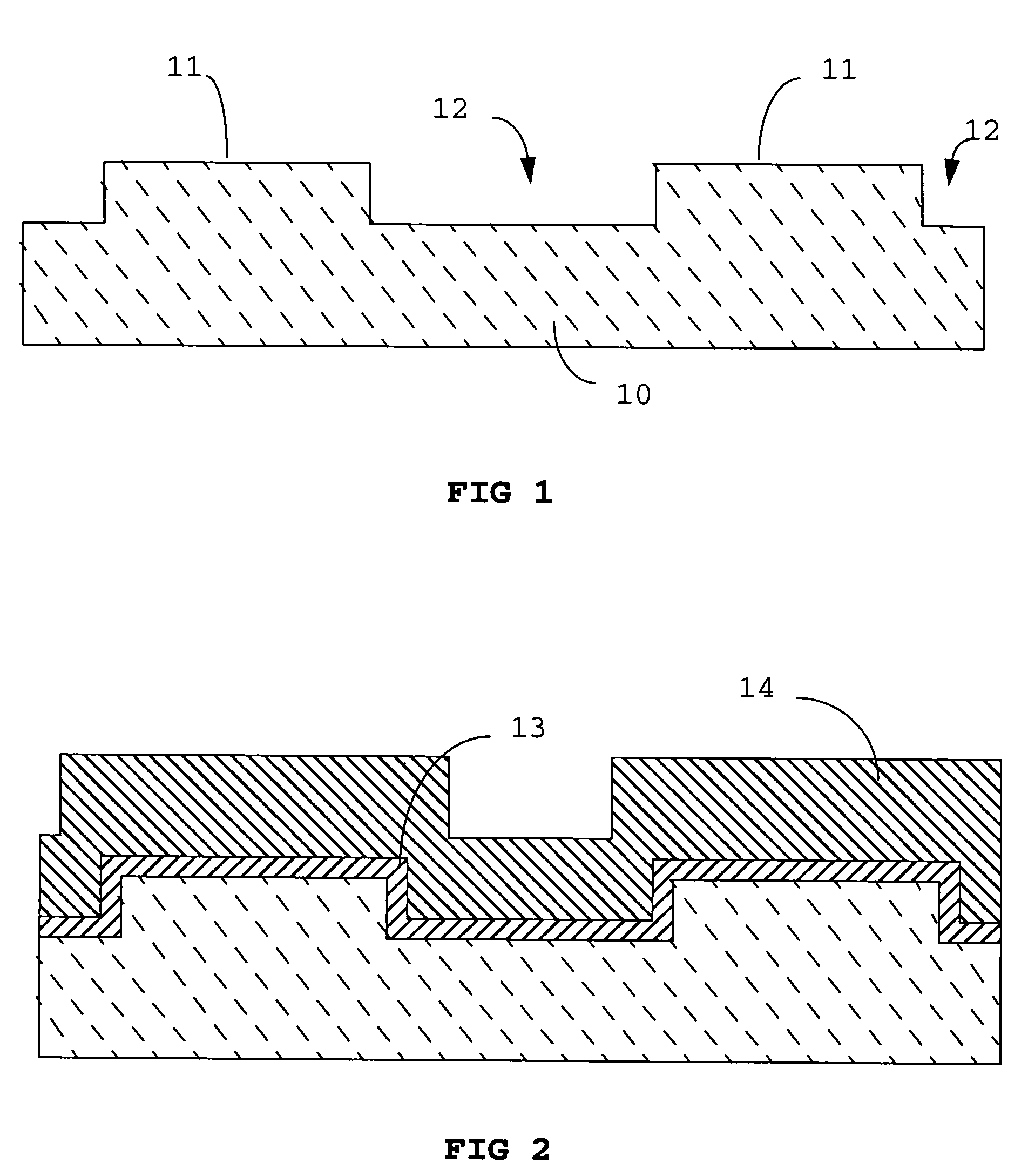
[0024] The GaAs wafer (10) shown in FIG. 1 is either semi-insulating (near intrinsic), or is doped of the opposite type to be used in the outer portions of the active regions (11).

[0025] The wafer is patterned with conventional photolithographic means, and an etch that leaves 500 A-5000 A deep isolation trenches in the GaAs. The FIG. 1 drawing shows sharp bottom corners, but the GaAs etch used at this step will need to round these corners to a degree dictated by the modulus of the gap fill material, and the temperature of subsequent anneals used.

[0026] An optional background implant may be done at this point.

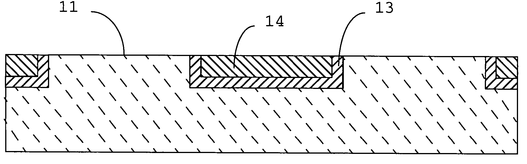
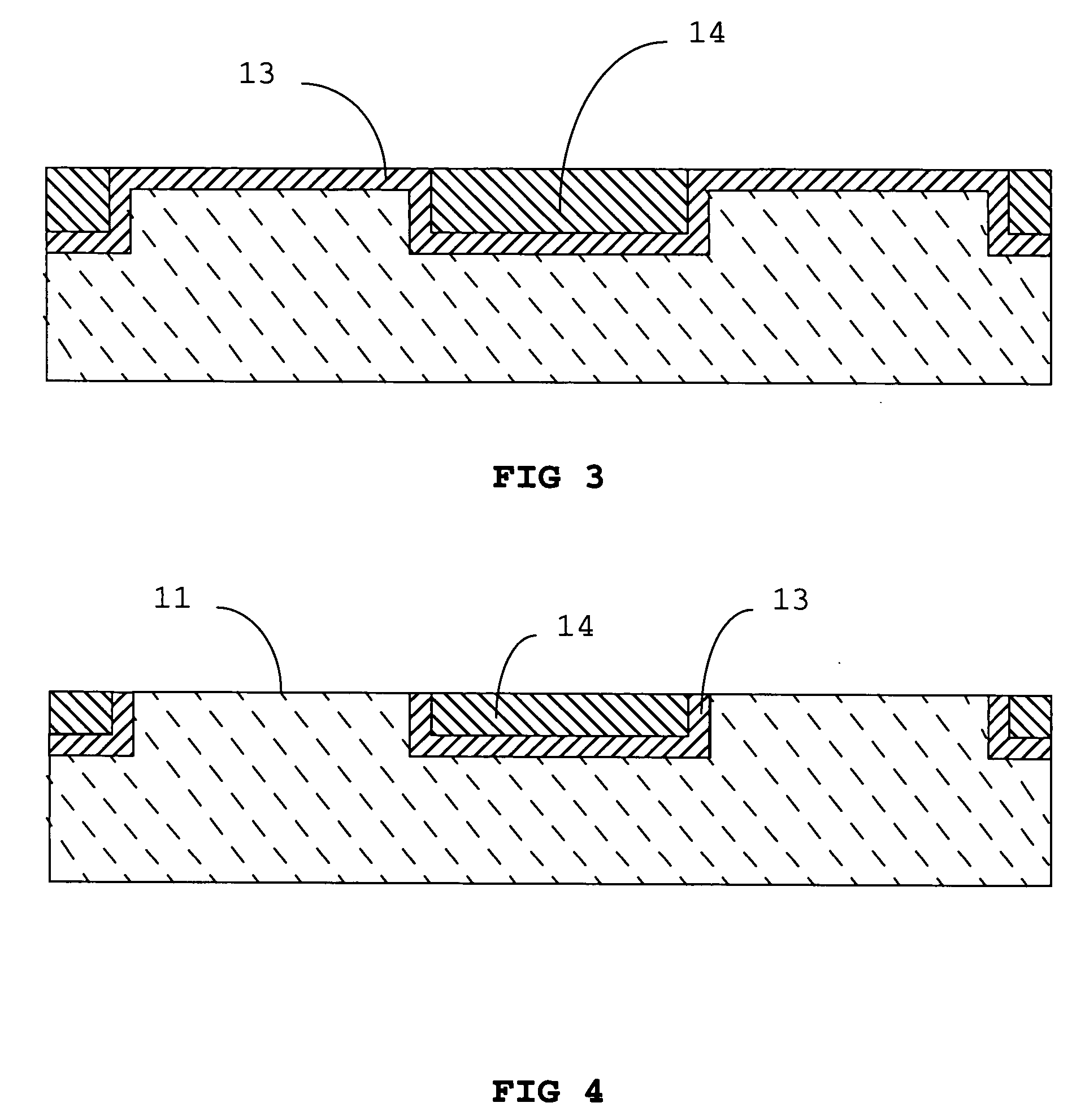
[0027] Next silicon nitride (13) is deposited on the semiconductor as a combination anneal cap layer, and a CMP stop layer. The thickness of this layer is typically 5-25% of the depth of the trench etched, but specifically depends on the uniformities and selectivities of the subsequent process steps.

[0028] A silicon dioxide gap fill layer (14) is deposited on top of the anne...

second embodiment

[0034] The GaAs wafer shown in FIG. 1 comprising a substrate, and device epitaxial layers grown on top. Device epitaxial layers may be those used for forming HBT devices, HEMT devices, optimized MESFET devices, or other devices.

[0035] To electrically isolate active regions of the wafers, the wafer is patterned with conventional photolithographic means, and an etch that removes the active layers of the wafer in the isolation regions (12). Depending on the epitaxial structure of the starting material, the depth of these trenches may be anywhere from 500 A to several microns.

[0036] Next, silicon nitride (13) is deposited on the semiconductor as a combination anneal cap layer, and a CMP stop layer. The thickness of this layer is typically 5-25% of the depth of the trench etched, but specifically depends on the uniformities and selectivities of the subsequent process steps.

[0037] A silicon dioxide gap fill layer (14) is deposited on top of the anneal cap layer at a thickness larger th...


PUM


Abstract

A structure with significant topography enhancements over the traditional composite dielectric structure is provided. Topography reduction at this level of the device structure significantly enhances critical dimension control of subsequent device patterns through reduced depth of focus requirements during lithography, and reduced over-etch requirements.

Description

CROSS-REFERENCE TO RELATED APPLICATIONS [0001] N / A STATEMENT REGARDING FEDERALLY SPONSORED RESEARCH OR DEVELOPMENT [0002] This Invention was not conceived, constructed, or tested during the performance of a government contract. REFERENCE TO SEQUENCE LISTING, A TABLE, OR A COMPUTER PROGRAM LISTING COMPACT DISK APPENDIX [0003] N / A BACKGROUND OF THE INVENTION [0004] 1. Field of Invention [0005] The present invention relates broadly to III-V semiconductor devices, and in particular, an improved isolation structure for such devices. [0006] 2. Description of the Prior Art [0007] The composite dielectric layer used in the fabrication of III-V devices, disclosed in U.S. Pat. No. 5,001,076, has been instrumental in yielding high levels of integration on such semiconductors. As transistor densities increase, and dimensions decrease, there becomes an increasing trade-off between the ability of the dielectric layer to mask ion implantations, and topography resulting from patterning of the compo...

Claims


Application Information

Patent Timeline
Patent Type & Authority Applications(United States)
IPC IPC(8): H01L21/76H01L21/8252H01L29/00
CPCH01L21/8252H01L21/7605
Inventor JOHNSON, DAVID ALANJURGENSEN, CHARLES W.
Owner JOHNSON DAVID ALAN
Why Eureka
Try Eureka