Sram cell fabrication with interlevel Dielectric planarization

a technology of dielectric planarization and sram cell, which is applied in the direction of electrical equipment, semiconductor devices, semiconductor/solid-state device details, etc., can solve the problems of high-temperature data loss of cells and excess static power consumption, and achieve accurate poly resistor patterning, reduce topography, and improve the degree of planarization

Inactive Publication Date: 2010-09-14
STMICROELECTRONICS SRL
View PDF43 Cites 0 Cited by
  • Summary
  • Abstract
  • Description
  • Claims
  • Application Information

AI Technical Summary

Benefits of technology

[0010]This disclosure describes an improved method of four transistor SRAM cell fabrication, wherein planarization is performed before metal formation (and actually before resistor formation). The pre-metal planarization utilizes a sandwich structure comprising permanent SOG, undoped glass, and permanent SOG. The undoped glass is used as a buffer layer between two layers of spin-on-glass to prevent SOG cracks. The double SOG spin enhances the degree of planarization.
[0011]The disclosed inventions thus provide the advantages of reduced topography at the poly-2 level, and hence more accurate patterning of the poly resistors, and hence a reduced poly-R resistance value by shortening resistor length (less surface contour due to better planarity). This provides more precise manufacturing control which can be used to set speed and power more reliably.BRIEF DESCRIPTION OF THE DRAWING

Problems solved by technology

Unfortunately, the resistivity of such polysilicon is fairly variable, and an excessive value for the resistors may cause the cell to lose data under high-temperature conditions.
An excessively low value for the polysilicon resistor may lead to excess static power consumption.

Method used


Image

  • Sram cell fabrication with interlevel Dielectric planarization
  • Sram cell fabrication with interlevel Dielectric planarization
  • Sram cell fabrication with interlevel Dielectric planarization

Examples


Embodiment Construction

[0019]The numerous innovative teachings of the present application will be described with particular reference to the presently preferred embodiment. However, it should be understood that this class of embodiments provides only a few examples of the many advantageous uses of the innovative teachings herein. In general, statements made in the specification of the present application do not necessarily delimit any of the various claimed inventions. Moreover, some statements may apply to some inventive features but not to others.

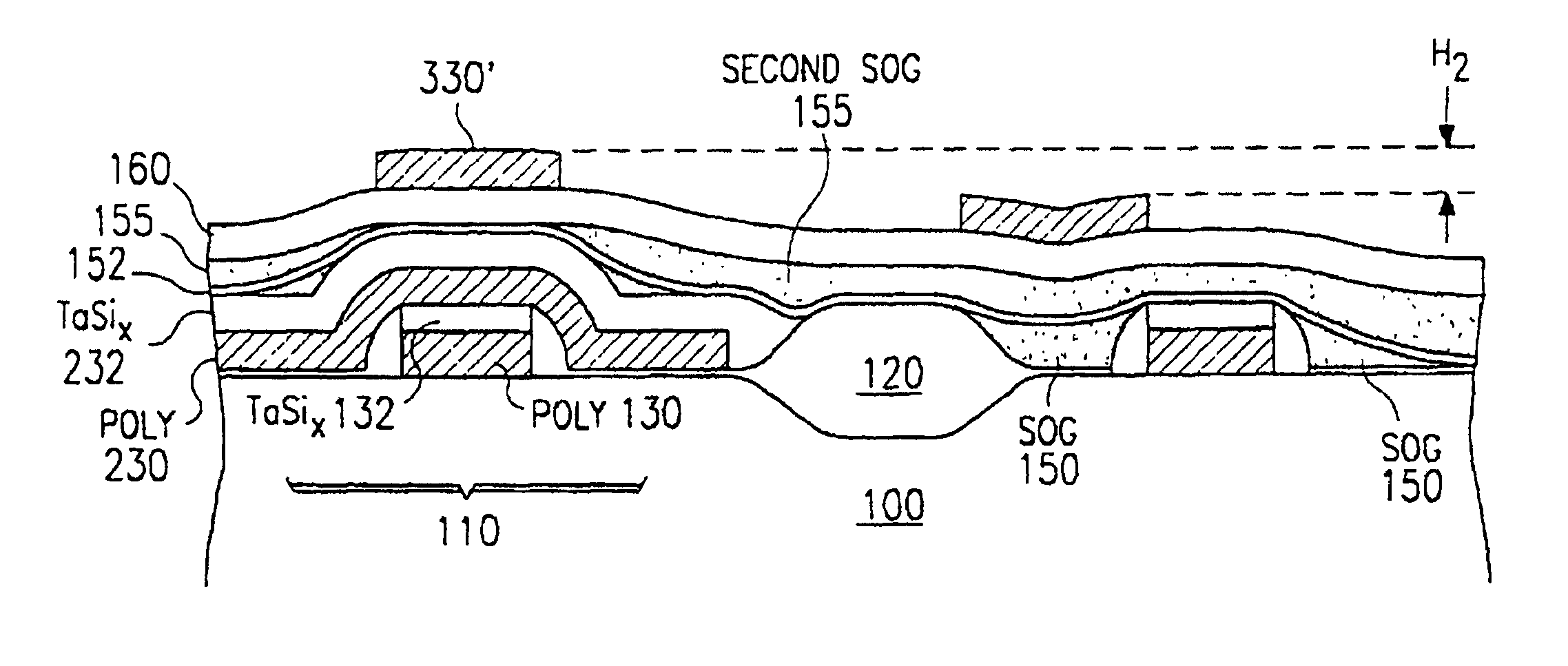
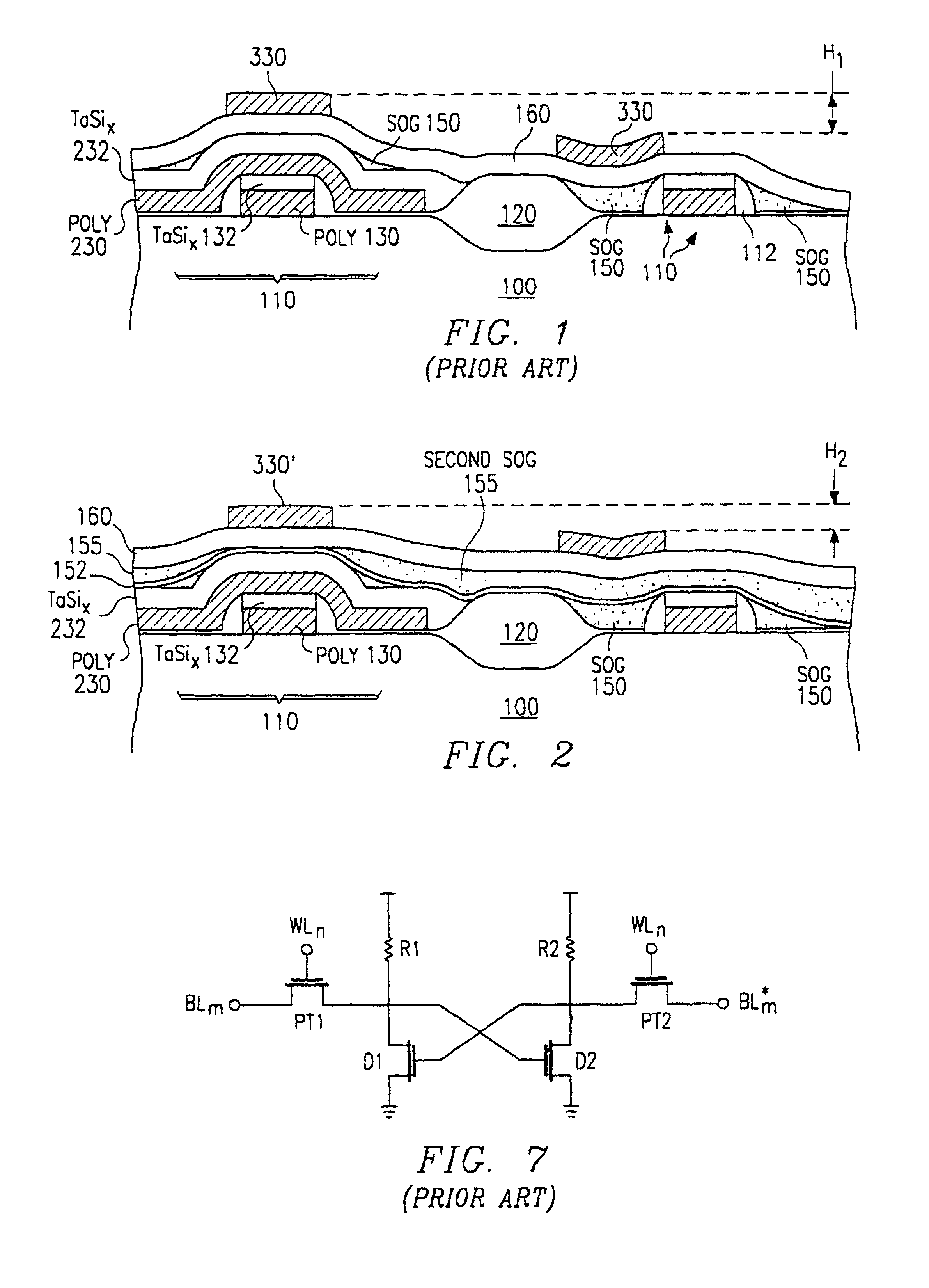
[0020]After completion of CMOS transistor formation (and local interconnect formation in the poly-2 layer, if desired), a standard process flow (as shown in FIG. 1) would deposit e.g. 1KÅ of undoped oxide, spin on e.g. 1.5KÅ of SOG, deposit e.g. 1KÅ of undoped oxide, deposit and etch a second polysilicon layer to form polysilicon resistors, and then proceed with contact and metal formation.

[0021]In the innovative process embodiments described, fabrication of th...


PUM


Abstract

A 4-T SRAM cell in which two layers of permanent SOG (with an intermediate oxide layer) are used to provide planarization between the first and topmost poly layers.

Description

[0001]This application is a continuation of application No. 08 / 328,736, filed Oct. 25, 1995, which was abandoned upon the filing herein which is a divisional of 08 / 49,338, filed Dec. 17, 1993, now U.S. Pat. No. 5,395,785.BACKGROUND AND SUMMARY OF THE INVENTION[0002]The present invention relates to integrated circuit fabrication methods and structures, and particularly to integrated circuits with minimum linewidths below one-half micron.[0003]Background: Planarization[0004]As the degree of integration has advanced, it has become increasingly apparently that it is desirable to minimize the topographical excursion of the surface at each level, especially the upper levels. To accomplish this, various planarization schemes have been used to planarize the inter-level dielectric. Some of these include Chemical-Mechanical-Polishing (CMP), use of Permanent Spin-on-glass (left in place in the final chip), and Sacrificial Etchback Spin-on-glass (SOG).[0005]Spin-on glass deposition is an exampl...

Claims


Application Information

Patent Timeline
Patent Type & Authority Patents(United States)
IPC IPC(8): H01L29/34H01L23/522H01L23/48H01L21/02H01L21/3105H01L21/70H01L21/768H01L21/8244
CPCH01L21/76819Y10S257/903Y10S257/904H10B10/15H10B10/00
Inventor NGUYEN, LOISUNDARESAN, RAVISHANKAR
Owner STMICROELECTRONICS SRL
Why Eureka
Try Eureka