

Probe card assembly including a programmable device to selectively route signals from channels of a test system controller to probes
a probe card and channel technology, applied in the direction of measurement devices, semiconductor/solid-state device testing/measurement, instruments, etc., can solve the problems of unreliable relays, insufficient channels, and significant cost factors of test system controllers with increased test channels, so as to achieve greater switching density, longer lifecycle, and reliable
- Summary
- Abstract
- Description
- Claims
- Application Information
AI Technical Summary
Benefits of technology
Problems solved by technology
Method used
Image

Examples
Embodiment Construction
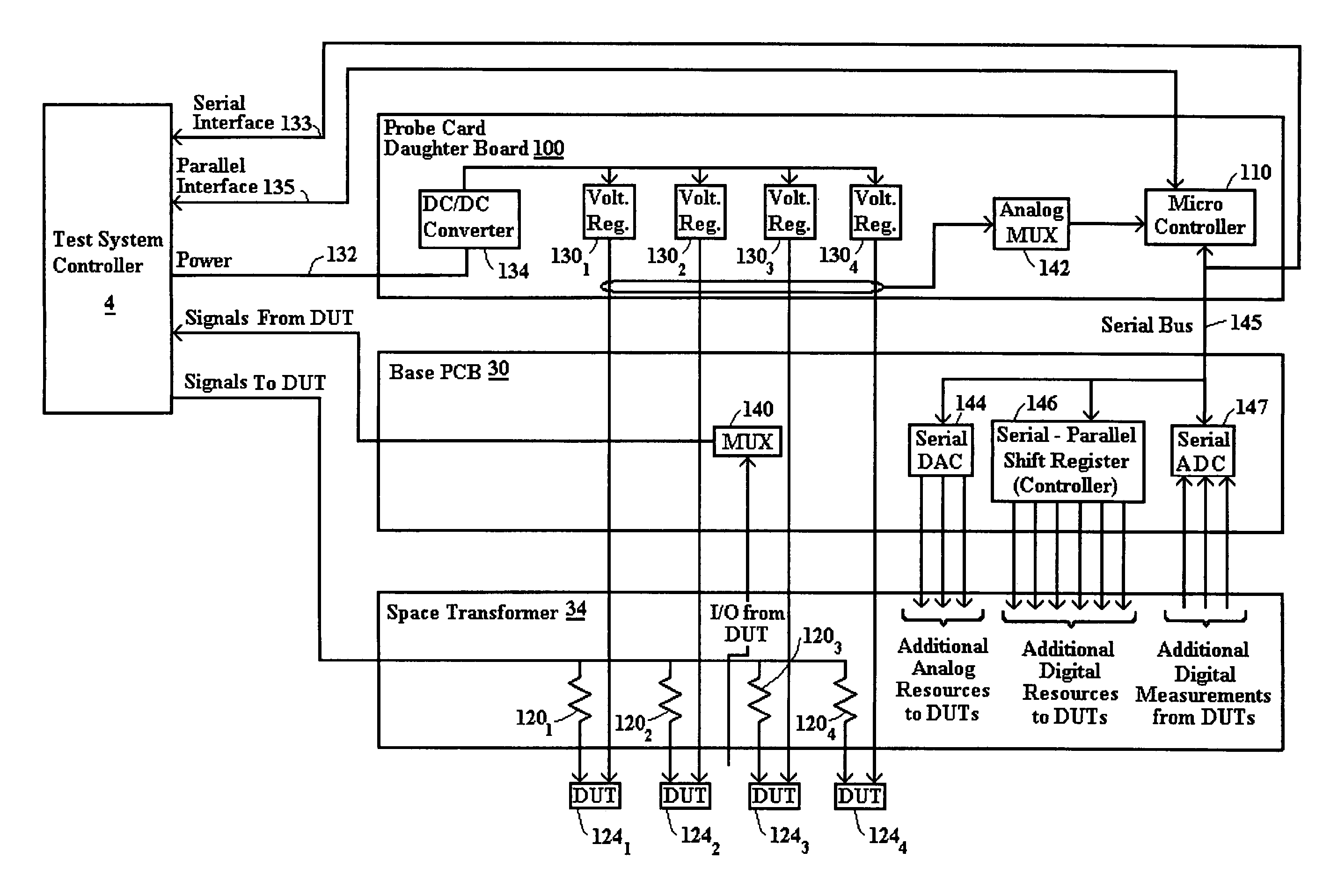
[0032]FIG. 6 shows a cross sectional view of a probe card, modified from the probe card configuration shown in FIG. 3 to include on board components, in accordance with the present invention, including daughter cards 100 and 102. For convenience, components carried over from FIG. 3 to FIG. 6 are similarly labeled. The daughter cards are shown in FIG. 6 as connected by stacked connectors 1041-4. The stacked connectors are attached to opposing card surfaces, and include male and female mating connectors. For example connector 1041 is connected to the base PCB 30, while connector 1042 is connected to daughter card 100. The stacked connectors can be ZIF, pogo pin, or other type connectors suitable for interconnecting printed circuit boards. The connectors make the daughter cards removable so that different daughter cards can be easily installed, depending on the test environment. Although shown with removable connectors, in one embodiment, the daughter cards can be rigidly connected, su...
PUM
 Abstract
Description
Claims
Application Information