Data output circuit with improved overvoltage/surge protection

a data output circuit and overvoltage protection technology, applied in logic circuit coupling/interface arrangement, pulse technique, baseband system details, etc., can solve the problems of undesirable failure of nmos transistors, inferior endurance of low-voltage transistors, etc., to achieve effective high-speed operation of data output circuits and efficient overvoltage and surge protection

Active Publication Date: 2007-07-17
RENESAS ELECTRONICS CORP
View PDF9 Cites 9 Cited by
  • Summary
  • Abstract
  • Description
  • Claims
  • Application Information

AI Technical Summary

Benefits of technology

[0017]Since the first and second P-channel MOS transistors provide overvoltage and surge protection for the first and second cascade MOS transistors, this architecture allows the first and second cascade MOS transistors to be composed of low-voltage transistors. Therefore, this architecture effectively achieves high-speed operation of the data output circuit with efficient overvoltage and surge protection.

Problems solved by technology

Although exhibiting high operation speed, low-voltage transistors suffer from inferior endurance against the overvoltage and surge.
Therefore, overvoltage and surge protection is an important issue for a CPU board incorporating data output circuits composed of low-voltage transistors.
This undesirably causes an overvoltage to be applied to the NMOS transistor 101, and may result in undesirable failure of the NMOS transistor 101 through the gate-oxide breakdown.
Additionally, due to the limitation of the rated operation voltage of the low-voltage transistors, the data output circuit shown in FIG. 1 can not output signal levels over the rated operation voltage of the NMOS transistors 101 and 102 even during the normal operation; this undesirably restricts the use of the data output circuit.
The use of high-voltage MOS transistors, such as multi-oxide transistors, for the NMOS transistors 101 and 102 within the data output circuit shown may achieve effective overvoltage and surge protection; however, this undesirably hinders high speed operation of the data output circuit due to the reduced gain of the high-voltage transistors.
Further, the use of high-voltage transistors undesirably necessitates a high power supply voltage to allow the data output circuit to operate at high speed.

Method used


Image

  • Data output circuit with improved overvoltage/surge protection
  • Data output circuit with improved overvoltage/surge protection
  • Data output circuit with improved overvoltage/surge protection

Examples


Embodiment Construction

[0026]The invention will be now described herein with reference to illustrative embodiments. Those skilled in the art would recognize that many alternative embodiments can be accomplished using the teachings of the present invention and that the invention is not limited to the embodiments illustrated for explanatory purposed.

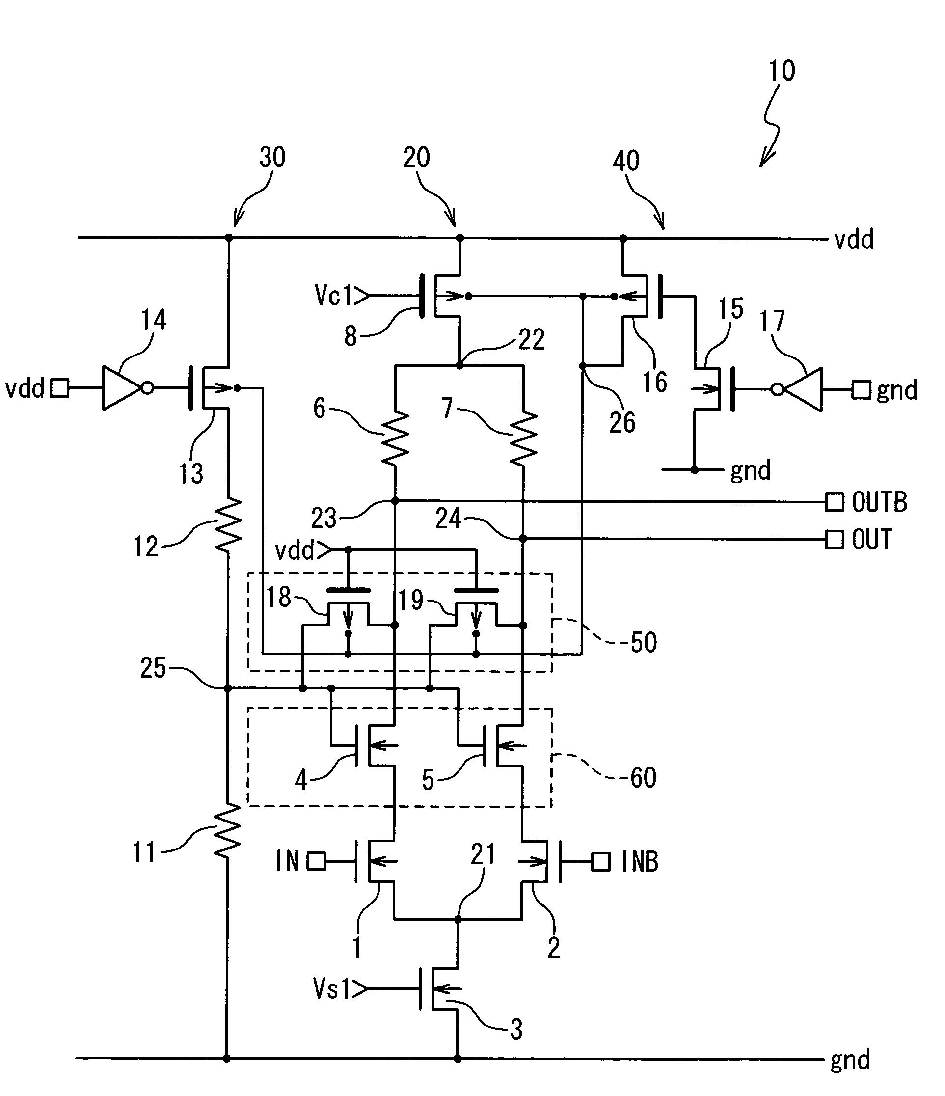
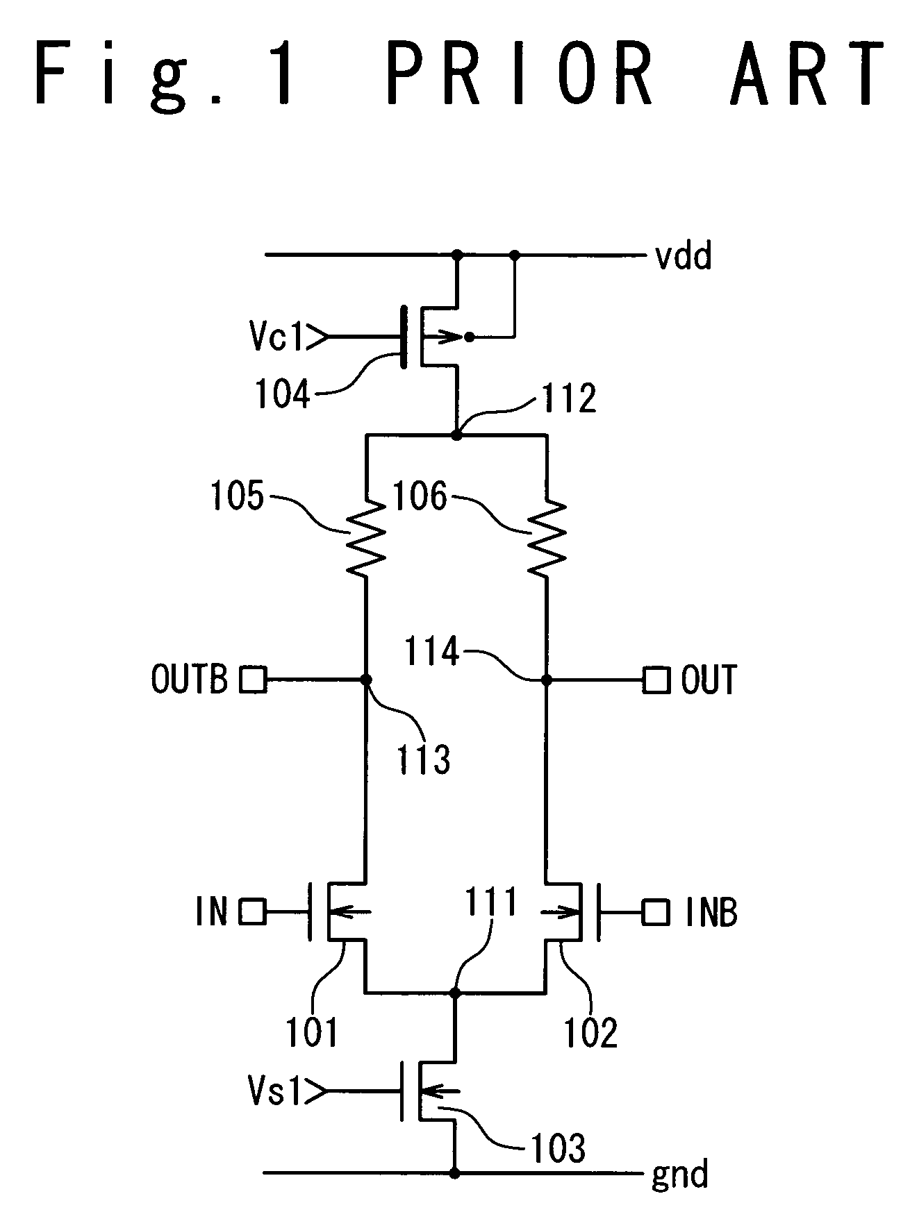
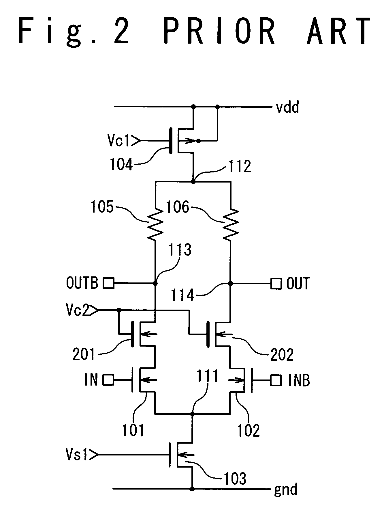
[0027]In this embodiment, the term “low-voltage transistor” means a MOS transistor adapted to operate on a low voltage as compared with the power supply voltage, exhibiting poor overvoltage and surge protection. In this embodiment, low voltage transistors are assumed to have a rated operation voltage of 1.3V, and an absolute maximum rating of 1.6V. Additionally the term “high-voltage transistor” means a transistor exhibiting improved overvoltage and surge protection as compared with the low voltage transistors.

[0028]FIG. 3 is a circuit diagram of a data output circuit 10 in this embodiment, which is adapted to operate on a power supply voltage of 3.6V. The data ...


PUM


Abstract

A data output circuit is composed of first and second differential MOS transistors, first and second cascade MOS transistors, first and second outputs, and first and second resistor elements. The first and second differential MOS transistors receive first and second input voltages on the gates, respectively, sources of the differential MOS transistors being commonly connected. The first cascade MOS transistor is connected between the first differential MOS transistor and the first output, and the second cascade MOS transistor is connected between the second differential MOS transistor and the second output, gates of the first and second cascade MOS transistors being commonly connected. The first transistor element is connected between a ground line and the commonly connected gates, and the second transistor element is connected between a power supply line and the commonly connected gates.

Description

BACKGROUND OF THE INVENTION[0001]1. Field of the Invention[0002]The present invention relates to data output circuits integrated within LSIs, such as data output buffer circuits. More specifically, the present invention relates to data output circuits suitable for outputting data on transmission lines through connection slots.[0003]2. Description of the Related Art[0004]The progress in semiconductor technologies has enhanced the use of high-performance computers in various applications. Computers are necessarily designed to be suitable for users' purposes. One approach for improving suitability of computers for users' purposes is to incorporate a set of CPU boards, each used for data processing, on a backplane board in a computer system, as disclosed in Japanese Laid-Open Patent Application No. H08-6676A.[0005]In order to achieve high-speed operation, high speed data transmission is required in the computer system. This necessitates high transmitting speed through data transmission ...

Claims


Application Information

Patent Timeline
Patent Type & Authority Patents(United States)
IPC IPC(8): H03K19/0175H03K19/003H03K17/08H03K17/0812H03K17/0814H03K17/10H03K17/687H03K19/0185H03K19/094H04L25/02
CPCH03K17/08142H03K17/102H03K19/00315H03K19/018528H04L25/028H04L25/0272
Inventor WATARAI, SEIICHI
Owner RENESAS ELECTRONICS CORP
Why Eureka
Try Eureka