
Semiconductor device

a technology of semiconductor devices and devices, applied in semiconductor devices, semiconductor/solid-state device details, electrical apparatus, etc., can solve the problems of deteriorating interconnect or similar integration density, reduced effective use area of elements, so as to improve interconnect density, high speed operability of elements, and effective utilization of upper regions

Active Publication Date: 2007-07-24
RENESAS ELECTRONICS CORP
View PDF9 Cites 18 Cited by
  • Summary
  • Abstract
  • Description
  • Claims
  • Application Information

AI Technical Summary

Benefits of technology

The present invention provides a semiconductor device with improved interconnect density and high speed operability of elements. The semiconductor device includes a first semiconductor chip with a first pad and a second semiconductor chip as a logic chip. The second semiconductor chip is connected to the first semiconductor chip via the first pad and the second pad. The second semiconductor chip has a multi-level interconnect layer with a through electrode connected to a conductive component provided within the multi-level interconnect layer and a second pad mounted on the top of the multi-level interconnect layer. This configuration allows for effective use area of the through electrode and improves interconnect density as compared with the related art. Additionally, the present invention suppresses delay of transmission of an electrical signal and achieves high speed operability of the logic chip.

Problems solved by technology

However, it has now been discovered that the through electrode of a configuration described in the related art is formed across the front surface from a rear surface of an element, therefore, there is a problem that an effective use area of the element is reduced.
That is, it is not possible to provide an interconnect or the like in the region where the through electrode is formed, therefore, the effective use area of the element is reduced, so that an integration density of the interconnect or the like deteriorates.
In the case of the logic chip that is intensely required to realize high density interconnect, the above mentioned problem becomes more serious.

Method used


Image

  • Semiconductor device
  • Semiconductor device
  • Semiconductor device

Examples


first embodiment

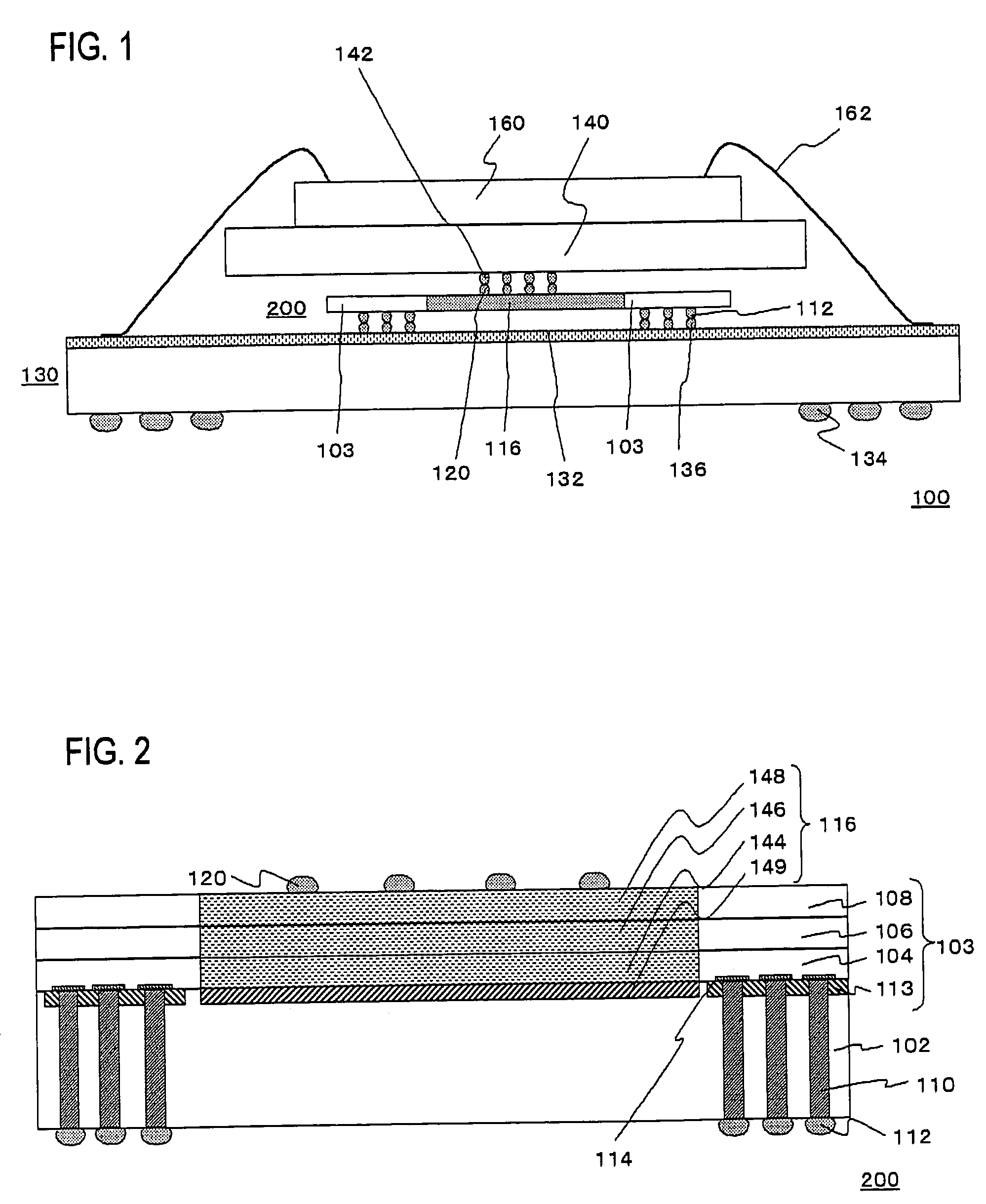
[0028]FIG. 1 is a cross-sectional view showing a configuration of a semiconductor package 100 according to the present embodiment.

[0029]The semiconductor package 100 is composed of a package substrate 130 as a circuit substrate, the logic chip 200, the DRAM 140, and a flash memory 160. Here, the front surface of the package substrate 130 is provided with an interconnect layer 132, and the rear surface of the package substrate 130 is provided with a bump 134. In addition, the interconnect layer 132 provided for the package substrate 130 is electrically connected to the logic chip 200 via the through electrode 110 or the like, which is described later. The logic chip 200 is electrically connected to the DRAM 140 via the bump 120 and a bump 142. Here, the bump 120 is mounted on the top of a logic circuit 116, which is described later. The flash memory 160 is mounted on the DRAM 140, and the flash memory 160 is electrically connected to the interconnect layer 132 provided for the packag...

second embodiment

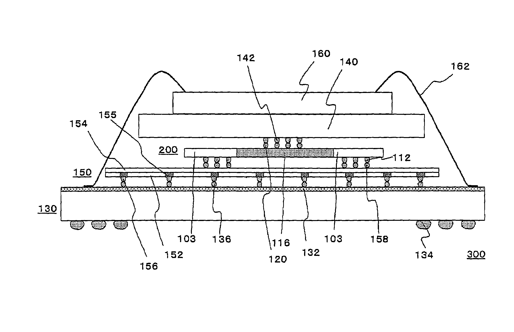
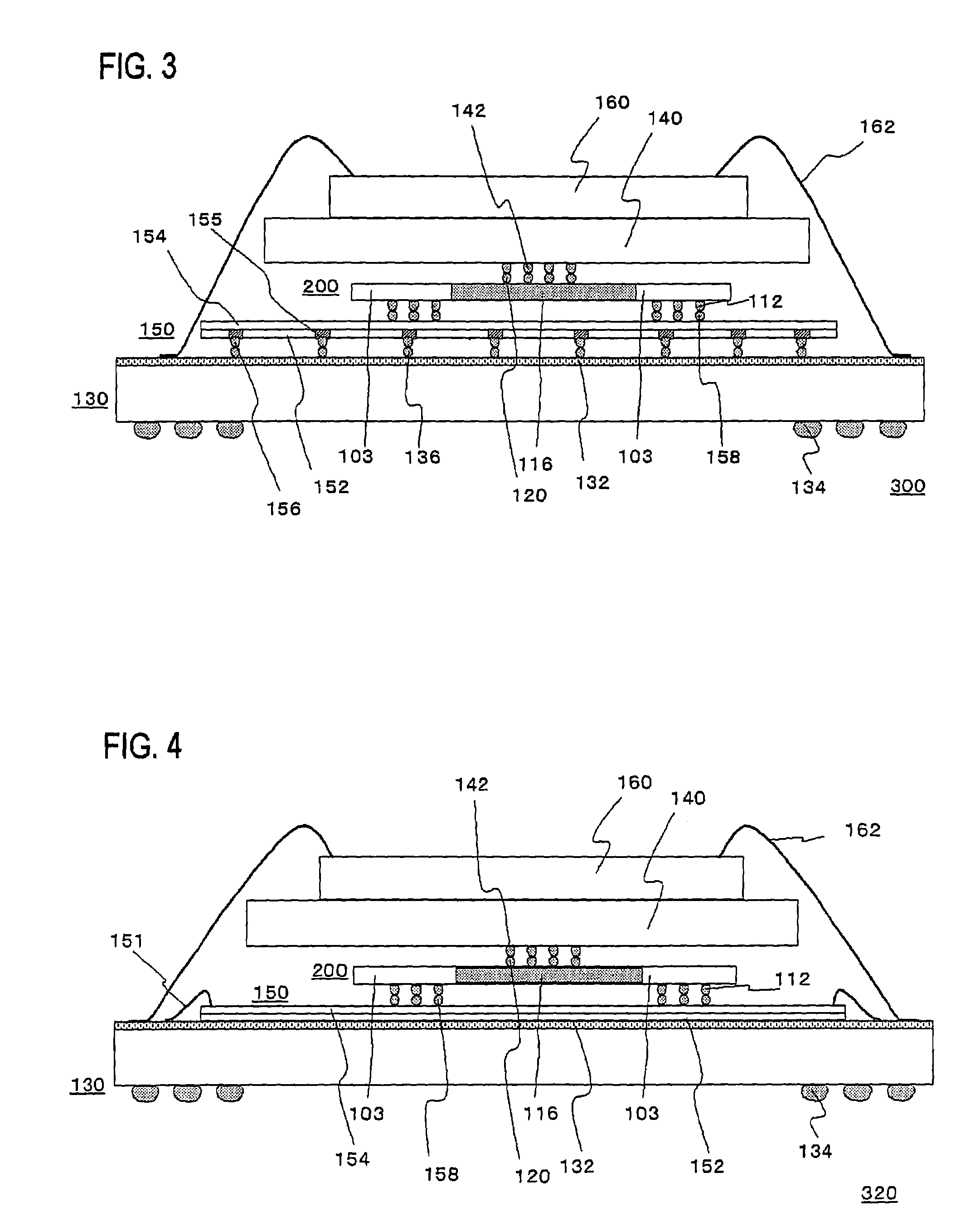
[0040]In the first embodiment, a configuration is that the interconnect layer 132 provided on the package substrate 130 is electrically connected to the logic chip 200 via the bump 136 and the bump 112, however, an interposer 150 may be provided between the package substrate 130 and the logic chip 200.

[0041]FIG. 3 is a cross-sectional view showing a configuration of a semiconductor package 300 according to the present embodiment.

[0042]The interconnect layer 132 provided on the package substrate 130 is electrically connected to the interposer 150 via the bump 136 provided on the front surface of the interconnect layer 132 and a bump 156 provided on a rear surface of a substrate 152 of the interposer 150. In addition, a through electrode 155 penetrates the substrate 152 of the interposer 150, and is electrically connected to an interconnect layer 154 of the interposer 150.

[0043]The interposer 150 is electrically connected to the logic chip 200 via a bump 158 provided on the front surf...

third embodiment

[0048]In the first embodiment and the second embodiment, the configuration is that the DRAM 140 is mounted on the logic chip 200, however, a configuration may also be suitable that the DRAM 140 is mounted on the package substrate 130 and the logic chip 200 is mounted on the DRAM 140.

[0049]FIG. 5 is a cross-sectional view showing a configuration of a semiconductor package 340 according to the present embodiment.

[0050]The DRAM 140 is mounted on the package substrate 130, the logic chip 200 is mounted on the DRAM 140, and the bump 112 mounted on the rear surface of the logic chip 200 is electrically connected to the interconnect layer 132 provided on the package substrate 130 with the gold wire 101.

[0051]Hereinafter, there will be described effects of the semiconductor package 340.

[0052]A circuit face (main surface) of the DRAM 140 is provided on the upper surface thereof; and a circuit face of the logic chip 200 is provided on the lower surface thereof. Therefore, an electrical connec...


PUM


Abstract

A semiconductor device, which is constituted in such a way that a pad portion of a logic chip is connected to an element region of a semiconductor chip with a bump bonding, is capable of achieving high speed operability of the elements, because delay of transmission of an electrical signal is suppressed a logic chip is directly connected to a DRAM, therefore, it is possible to suppress an increase of load capacitance caused by interconnects, and securing a wide bus width by a multiple pin connection. As a result, it becomes possible to enhance performance of the semiconductor device upon suppressing delay of information transmission from the logic chip to the DRAM.

Description

[0001]This application is based on Japanese patent application NO. 2004-081743, the content of which is incorporated hereinto by reference.BACKGROUND OF THE INVENTION[0002]1. Field of the Invention[0003]The present invention related to a semiconductor device formed with layered semiconductor chips.[0004]2. Related Art[0005]In recent years a semiconductor device is required to be lightweight, thin, and short sized, and a high performance. In the semiconductor device such as a multi-chip package or the like, realizing high density interconnect, miniaturization of a logic chip and capacity increase of a memory is aggressively promoted.[0006]As one corresponding medium coping with such requirements, it is tried that realizing high density interconnect or the like is achieved upon providing a through electrode on the semiconductor substrate. The Japanese Laid-Open Patent Publication No. 2000-12618 discloses this kind of technology. As shown in FIG. 10, the Japanese Laid-Open Patent Publi...

Claims


Application Information

Patent Timeline
Patent Type & Authority Patents(United States)
IPC IPC(8): H01L23/02H01L25/18H01L21/00H01L21/60H01L23/31H01L23/48H01L23/50H01L25/065H01L25/07
CPCH01L23/3128H01L25/0657H01L23/481H01L2224/16145H01L2224/48091H01L2224/48227H01L2225/0651H01L2225/06513H01L2225/06541H01L2225/06555H01L2924/01078H01L2924/01079H01L2924/15311H01L2924/19041H01L2924/00014H01L2224/45144H01L2924/00H01L24/48H01L24/16H01L24/45H01L2224/05001H01L2224/05026H01L2224/05624H01L2224/05644H01L2224/05647H01L2224/05655H01L2224/13025H01L2224/05099
Inventor KAWANO, MASAYA
Owner RENESAS ELECTRONICS CORP
Learn More