Magnetic sensing device, method of forming the same, magnetic sensor, and ammeter

a technology of magnetic sensing and ammeter, which is applied in the field of magnetic sensing devices, method of forming the same, magnetic sensors, and ammeters, can solve the problems of unpreferable increase in 1/f noise, and achieve the effects of stable sensing, suppressing the appearance of hysteresis, and high sensitivity

Active Publication Date: 2007-07-24
TDK CORPARATION
View PDF25 Cites 66 Cited by
  • Summary
  • Abstract
  • Description
  • Claims
  • Application Information

AI Technical Summary

Benefits of technology

[0014]The present invention has been achieved in consideration of such problems and its first object is to provide a magnetic sensing device capable of stably sensing a signal magnetic field at high sensitivity by suppressing appearance of a hysteresis to thereby reduce 1 / f noise, and a method of forming the same. A second object of the invention is to provide a magnetic sensor and an ammeter each including such a magnetic sensing device.

Problems solved by technology

Increase in the 1 / f noise is unpreferable since it is a big factor of deteriorating the reliability of the whole system.

Method used


Image

  • Magnetic sensing device, method of forming the same, magnetic sensor, and ammeter
  • Magnetic sensing device, method of forming the same, magnetic sensor, and ammeter
  • Magnetic sensing device, method of forming the same, magnetic sensor, and ammeter

Examples


first embodiment

[0062]First, the configuration of a magnetic sensing device as a first embodiment of the invention will be described with reference to FIGS. 1A to 1C to FIG. 5.

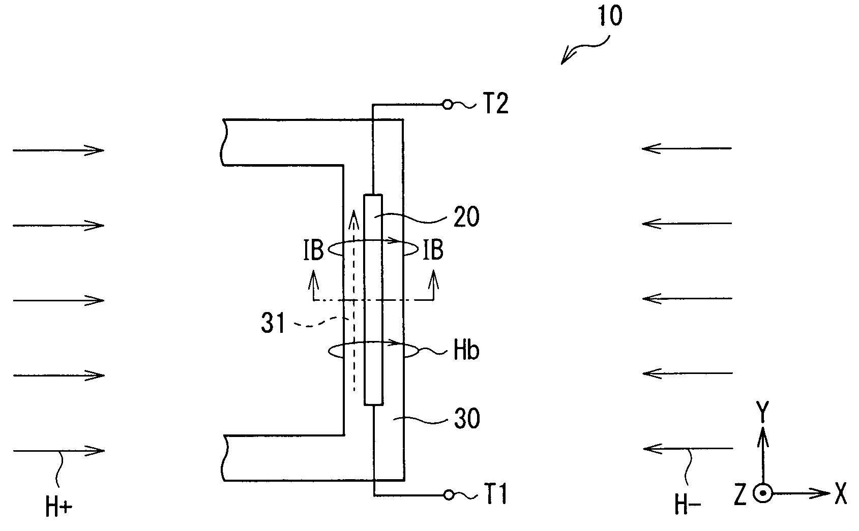
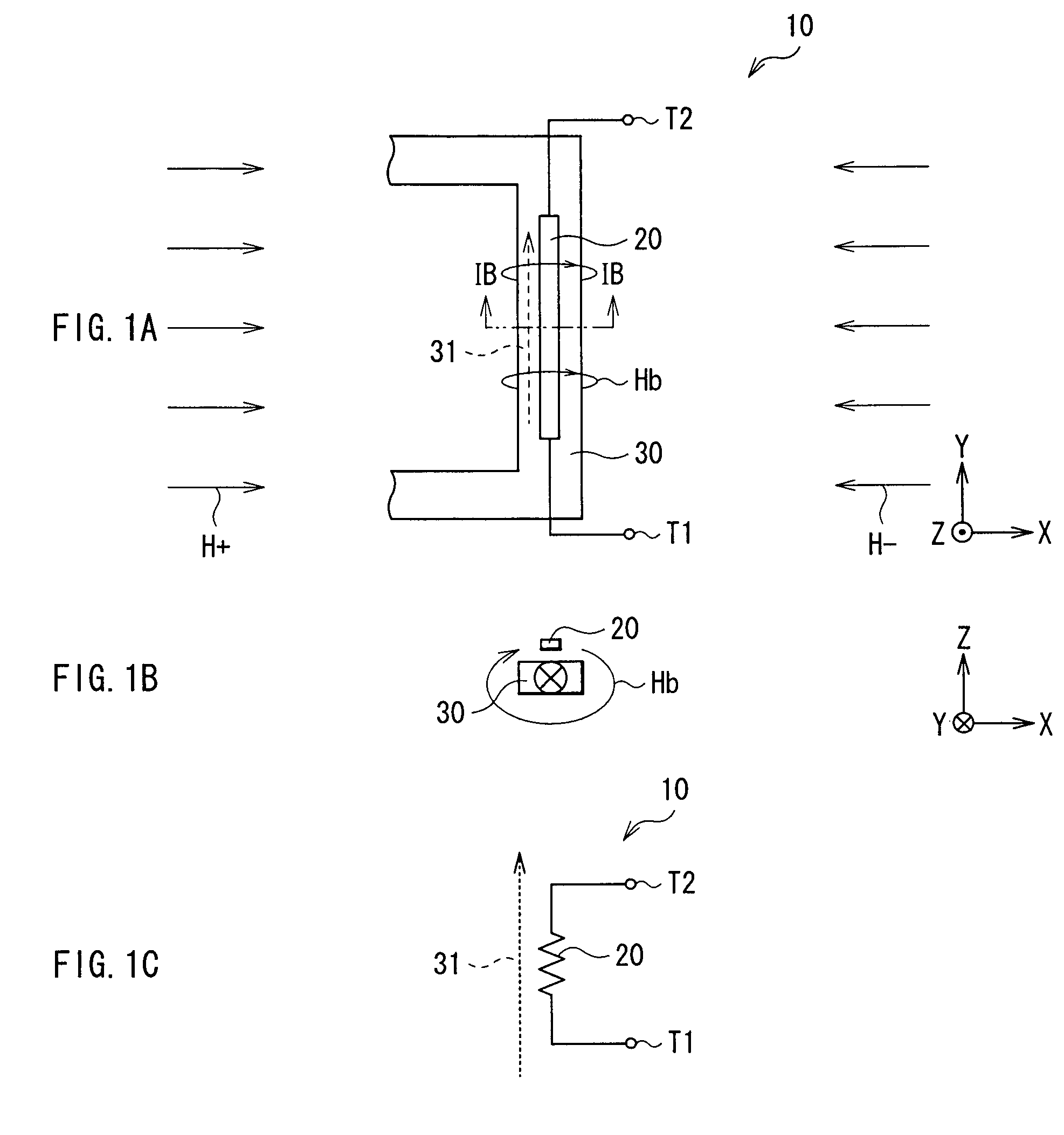
[0063]FIGS. 1A to 1C show a schematic configuration of a magnetic sensing device 10 of the first embodiment. FIG. 1A is a plan view showing the configuration of the magnetic sensing device 10 and FIG. 1B shows a sectional configuration of the magnetic sensing device 10, taken along the line IB-IB of FIG. 1A. FIG. 1C shows an equivalent circuit corresponding to FIG. 1A. The magnetic sensing device 10 senses the presence / absence of a magnetic field in the environment of the magnetic sensing device 10 (external magnetic field) and the intensity of the magnetic field.

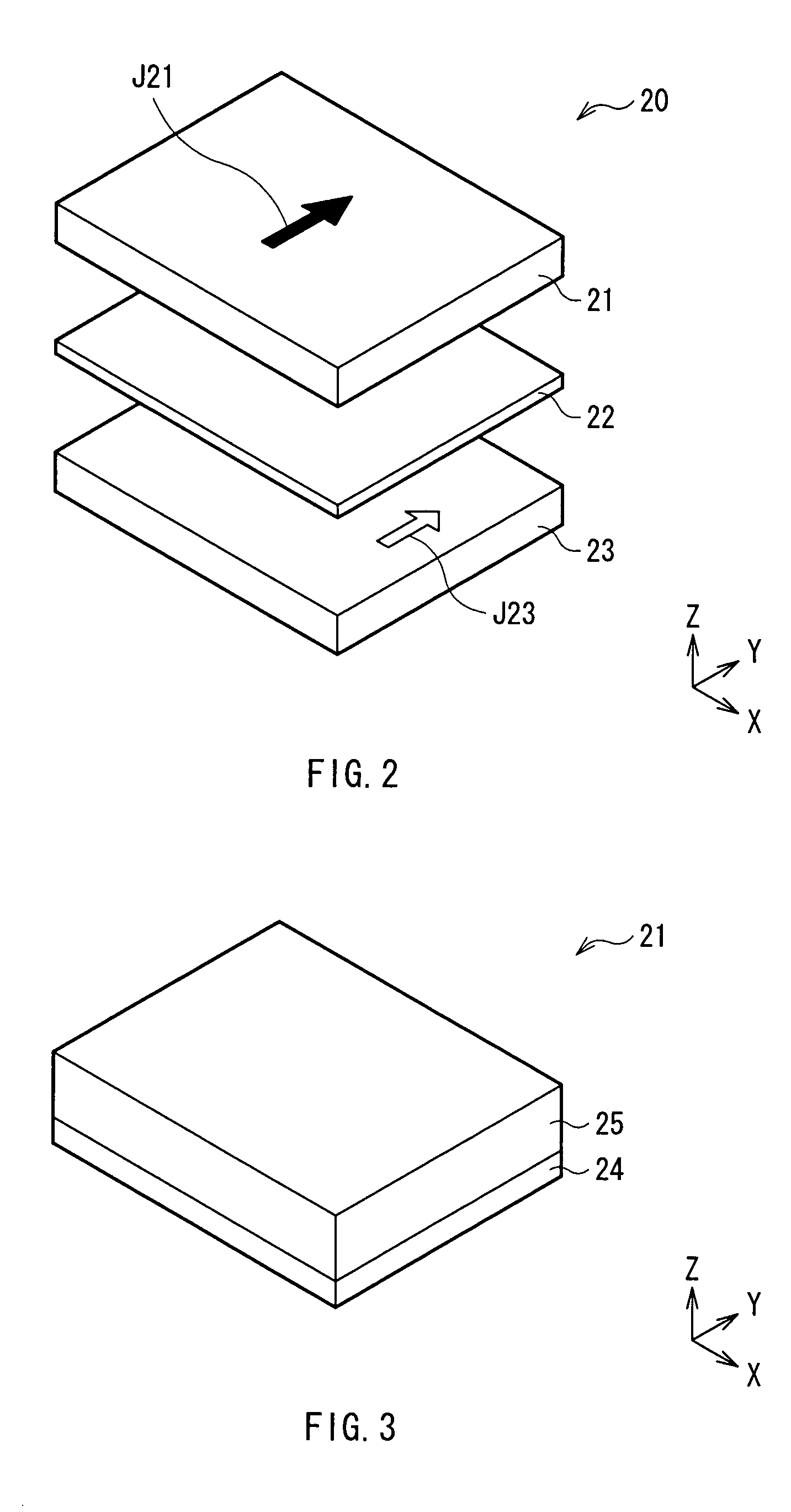
[0064]As shown in FIG. 1A, in the magnetic sensing device 10, a stacked body 20 and a bias current line 30 as bias applying means provided adjacent to the stacked body 20 are formed on a not-shown board. The stacked body 20 has a pinned layer whose magnetization dire...

second embodiment

[0078]Referring now to FIG. 9, as a second embodiment of the invention, the configuration of a magnetic sensor (ammeter) using the magnetic sensing device of the invention described in the first embodiment will be described.

[0079]FIG. 9 shows a schematic configuration of a magnetic sensor 1 of the invention.

[0080]The magnetic sensor 1 shown in FIG. 9 is an ammeter for detecting a magnetic field to be sensed which is generated by current to be sensed flowing in parallel or anti-parallel to the magnetization direction of a pinned layer. The magnetic sensor 1 has a first magnetic sensing module (hereinbelow, simply called a first module) 11 constructed by first and second magnetic sensing devices 10A and 10B connected to each other at a first connection point P1 and a second magnetic sensing module (hereinbelow, simply called a second module) 12 constructed by third and fourth magnetic sensing devices 10C and 10D connected to each other at a second connection point P2. The first and se...

first modification

[0095]FIG. 11 shows the configuration of a magnetic sensor 1A as a first modification. In the magnetic sensor 1A, like in the magnetic sensor 1, a bridge circuit is constructed by the first and second modules 11 and 12 formed on the same substrate (substrate 40). The magnetic sensor 1A, however, is different from the magnetic sensor 1 with respect to the point that the first and second magnetic sensing devices 10A and 10B are disposed diagonally, and the third and fourth magnetic sensing devices 10C and 10D are disposed diagonally. Specifically, the first and third magnetic sensing devices 10A and 10C are disposed on the same straight line extending in the direction corresponding to the magnetization directions J21A and J21C, and the second and fourth magnetic sensing devices 10B and 10D are disposed in the same straight line extending in the direction corresponding to the magnetization directions J21B and J21D. The relation between each stacked body 20 and the direction of each bia...


PUM

PropertyMeasurementUnit
temperatureaaaaaaaaaa
bias currentaaaaaaaaaa
magnetizationaaaaaaaaaa

Abstract

The present invention provides a magnetic sensing device capable of stably sensing a signal magnetic field with high sensitivity by suppressing occurrence of a hysteresis to reduce 1 / f noise. A magnetic sensing device has a stacked body including a pinned layer having a magnetization direction pinned to a predetermined direction (Y direction), a free layer having a magnetization direction which changes according to an external magnetic field and, when the external magnetic field is zero, becomes parallel to the magnetization direction of the pinned layer, and an intermediate layer sandwiched between the pinned layer and the free layer. Consequently, as compared with the case where the pinned layer and the free layer have magnetization directions which are orthogonal to each other when the external magnetic field is zero, variations in the spin directions of magnetic domains in the free layer can be reduced. In the case of passing read current, appearance of a hysteresis in the relation between a change in the external magnetic field and a resistance change can be suppressed. As a result, 1 / f noise is suppressed and a signal magnetic field can be stably sensed with high sensitivity.

Description

BACKGROUND OF THE INVENTION[0001]1. Field of the Invention[0002]The present invention relates to a magnetic sensing device capable of sensing a change in a signal magnetic field at high sensitivity, method of forming the same, a magnetic sensor having the magnetic sensing device, and an ammeter having the magnetic sensing device.[0003]2. Description of the Related Art[0004]Generally, a magnetic recording / reproducing apparatus for writing / reading magnetic information to / from a recording medium such as a hard disk has a thin film magnetic head including a magnetic recording head and a magnetic reproducing head. The reproducing head has a giant magneto-resistive effect element (hereinbelow, GMR element) executing reproduction of a digital signal as magnetic information by using so-called giant magneto-resistive effect.[0005]The GMR element used for a thin film magnetic head generally has a spin valve structure as shown in FIG. 19. Concretely, the GMR element is a stacked body 120 inclu...

Claims


Application Information

Patent Timeline
Patent Type & Authority Patents(United States)
IPC IPC(8): G01R33/02G01R15/20G01R33/09G11B5/39H01F10/32H01F41/30H01L43/08H01L43/10
CPCB82Y25/00G01R33/093G11B5/3903H01F10/3268H01F41/302G01R15/205
Inventor SHOJI, SHIGERU
Owner TDK CORPARATION
Why Eureka
Try Eureka