Array optical sub-assembly

a technology of optical sub-assembly and array, applied in the direction of optics, optical elements, instruments, etc., can solve the problems of reducing the overall performance of the optical sub-assembly, the inability to achieve the desired optical coupling efficiency and reliability, and the importance of optical data communication between the two, so as to reduce the difficulty of fabrication and improve the overall performance

Inactive Publication Date: 2007-07-31
IND TECH RES INST
View PDF11 Cites 4 Cited by
  • Summary
  • Abstract
  • Description
  • Claims
  • Application Information

AI Technical Summary

Benefits of technology

[0006]In view of the aforesaid problems, the primary object of the invention is to provide an array optical sub-assembly that has a novel structure with a separate photoelectric element and IC to reduce fabrication difficulties and improve overall performance.
[0007]In order to achieve the foregoing object, the array optical sub-assembly according to the invention includes a base seat, an IC, a transparent substrate and a photoelectric element. The base seat has a holding surface for holding one or more IC. The IC is mounted onto the holding surface. The transparent substrate covers the holding surface to form a sealed space with the base seat to protect the elements housed in the seal space. The photoelectric element is bonded to one side of the transparent substrate where the seal spaced is formed. The photoelectric element and the IC are spaced by a layer of air to prevent thermal interference between the photoelectric element and the IC. The photoelectric element is electrically connected to the IC through the transparent substrate and the base seat.
[0008]In addition, the invention further includes a microlens array on another side of the transparent substrate corresponding to the photoelectric element to increase the optical coupling efficiency of the photoelectric element.

Problems solved by technology

When computer and communication techniques are coupled, optical connections and optical data communication between them become important issues.
Such an approach does not produce desired optical coupling efficiency and reliability.
But alignment of the polymer microlens and other photoelectric elements is difficult.
However, such a technique involves soldering the photoelectric element directly onto the IC.
When the IC is in operation, the heat generated by the IC is transferred directly to the photoelectric elements and impairs signal transmission quality.
The technique also does not deal with how to package the integrated IC and photoelectric elements.
Packaging to meet reliability requirements is also a challenge.
However, it also has the same reliability and cooling problems encountered in U.S. Pat. No. 6,754,407.

Method used


Image

  • Array optical sub-assembly
  • Array optical sub-assembly
  • Array optical sub-assembly

Examples


Embodiment Construction

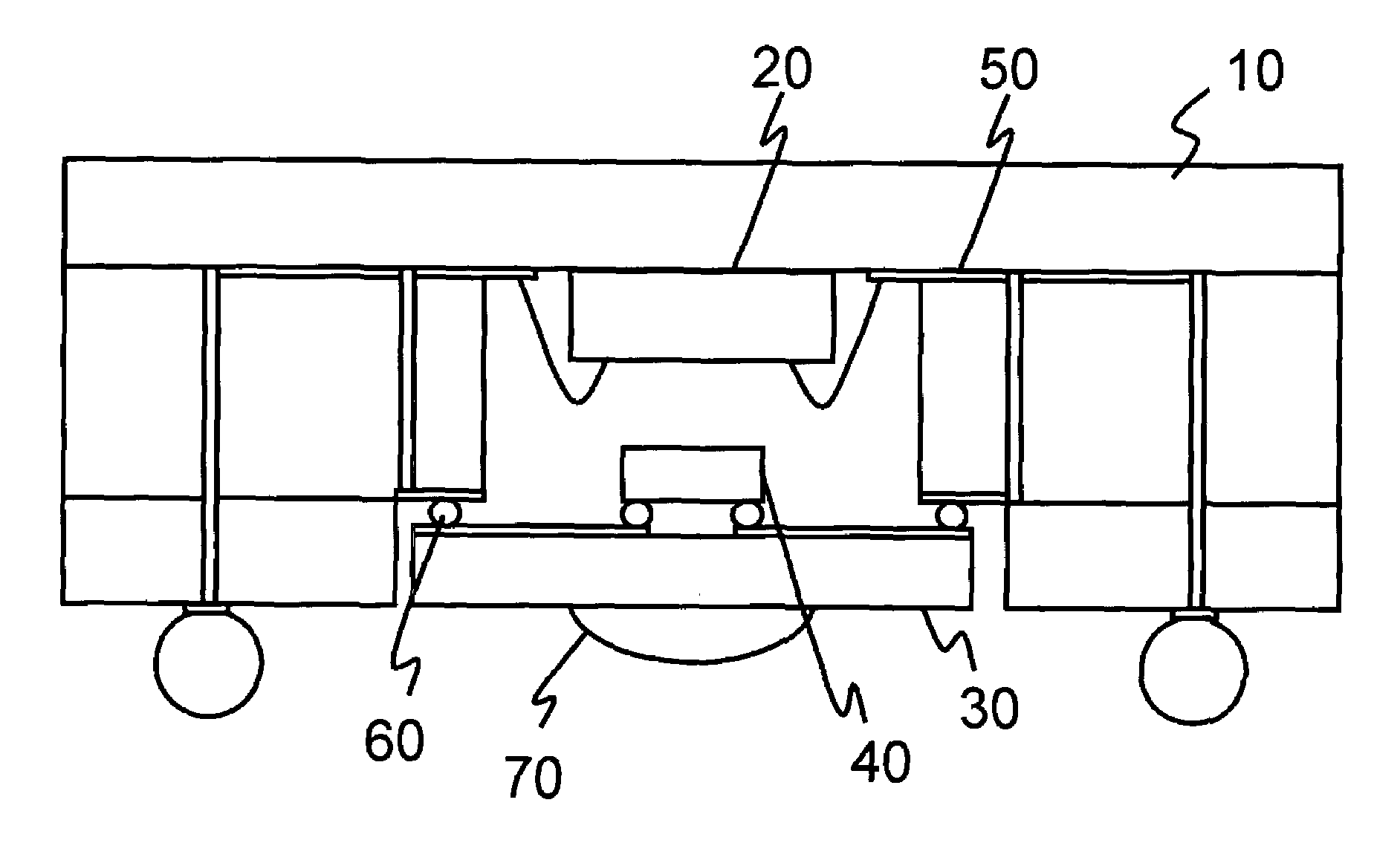
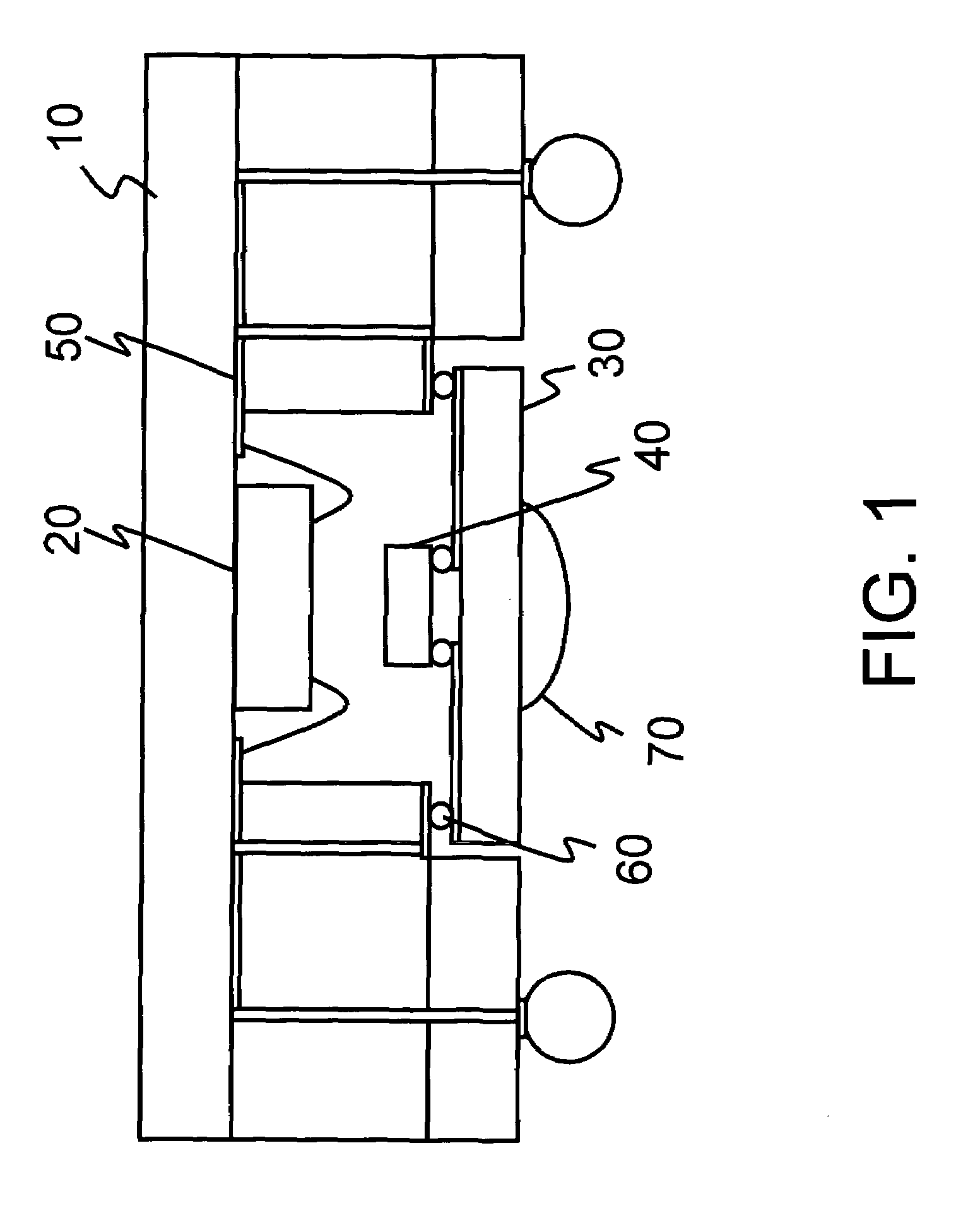
[0012]Refer to FIG. 1 for the structure of an embodiment of the array optical sub-assembly of the invention. It includes a base seat 10, an integrated circuit (IC) 20, a transparent substrate 30 and a photoelectric element 40. The base seat 10 has a holding surface for holding the IC 20. The IC 20 is mounted onto the holding surface, and has one or more sets. The transparent substrate 30 is coupled with the photoelectric element 40 and covers the holding surface of the base seat 10 to form a sealed or even airtight space with the base seat 10 to house the photoelectric element 40 and the IC 20. The photoelectric element 40 and the IC 20 are spaced from each other, so heat generated by the IC 20 does not directly transfer to the photoelectric element 40 and cooling problems may be mitigated.

[0013]The base seat 10 is made from ceramic material such as aluminum nitride (AIN) and aluminum oxide (Al2O3), or metal, plastics or polymer materials. The base seat 10 has a plurality of metal c...


PUM


Abstract

An array optical sub-assembly includes a base seat, an integrated circuit, a transparent substrate and a photoelectric element. The integrated circuit and the photoelectric element are bonded respectively to the base seat and the transparent substrate. The base seat and the transparent substrate form a sealed space to protect the elements. The photoelectric element and the integrated circuit are separated to avoid thermal interference between the photoelectric element and the integrated circuit. Therefore total performance is increased and fabrication difficulty is reduced.

Description

FIELD OF THE INVENTION[0001]The invention relates to an array optical sub-assembly and particularly to an array type optical sub-assembly that aims to facilitate manufacturing and production, and improve the optical coupling efficiency of photoelectric devices.BACKGROUND OF THE INVENTION[0002]To meet the requirements of high-speed broadband communication, optical communication industries that utilize light as a transmission medium have progressed rapidly. Optical fiber applications related to optical communication have also become increasingly important. To achieve the objectives of high-speed optical communication and expanded utilization, low cost optical communication devices and high speed transceiver modules are essential. Moreover, future development of data communication for high performance computers aims to employ optical interconnect to link computer chip sets, modules, circuit boards, base boards, cases and processors, and high speed photons for signal transmission to ove...

Claims


Application Information

Patent Timeline
Patent Type & Authority Patents(United States)
IPC IPC(8): G02B6/36G02B6/42G02B6/00
CPCG02B6/425H01L27/14618H01L27/14625H01L27/14627H01L27/14634H01L27/14685G02B6/4206H01L25/167H01L33/58H05K1/141H05K1/183H01L2224/48091H01L2224/48227H01L2924/00014H01L2224/16225H01L2924/00011H01L2224/0401
Inventor CHEN, YI-MINGCHEN, YING-CHIHCHENG, YAO-LINGLEE, SHUN-TIEN
Owner IND TECH RES INST
Why Eureka
Try Eureka