Insulated gate bipolar transistor

Inactive Publication Date: 2007-07-31
MITSUBISHI ELECTRIC CORP
View PDF12 Cites 28 Cited by
  • Summary
  • Abstract
  • Description
  • Claims
  • Application Information

AI Technical Summary

Benefits of technology

[0027]In the insulated gate bipolar transistor of the first aspect of the present invention, the selective formation of the first doped regions in the third main surface of the second semiconductor layer without being connected to the first semiconductor layer makes the effective concentration of the second semiconductor layer on the first doped regions lower. If the first conductivity type is an n type and the second conductivity type is a p type, the number of holes injected from the second semiconductor layer is reduced when the emitter electrode and the gate electrode are placed at the same potential and a higher potential is applied to the collector electrode than to the emitter and gate electrodes (in the off state). Consequently, the leakage current is reduced.
[0028]The non-connection of the first doped regions to the first semiconductor layer prevents a parasitic diode from being formed when connection is established between the first doped regions and the first semiconductor layer. Therefore, the insulated gate bipolar transistor of the first aspect can perform a stable operation when used in an inverter and the like.
[0029]The second semiconductor layer does not include a partially formed lower impurity concentration region. In other words, the second semiconductor layer has a substantially uniform impurity concentration. If the first conductivity type is the n type and the second conductivity type is the p type, electron currents flowing from the emitter electrode side at turn-off flow into the collector electrode uniformly. This suppresses the abrupt decay of the tail current in the collector current resulting from the partial formation of the lower impurity concentr

Problems solved by technology

The first background art IGBT having the above-mentioned structure is disadvantageous in that a large number of holes injected from the collector layer 90 which is the p+ semiconductor layer in an off state make an off-state leakage current (referred to simply as a “leakage current” hereinafter) high at elevated temperatures.
In particular, the first

Method used


Image

  • Insulated gate bipolar transistor
  • Insulated gate bipolar transistor
  • Insulated gate bipolar transistor

Examples


first preferred embodiment

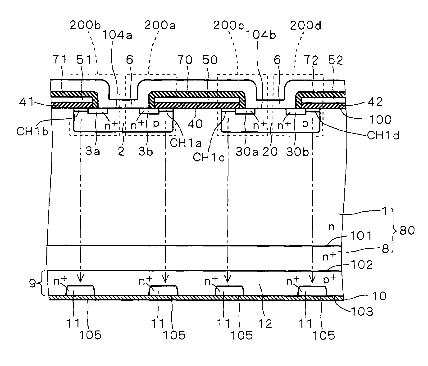
[0043]FIG. 1 is a schematic sectional view showing a structure of an IGBT according to a first preferred embodiment of the present invention. As shown in FIG. 1, the IGBT according to the first preferred embodiment comprises an n semiconductor layer 1 serving as an n type semiconductor substrate. An n+ buffer layer 8 having an impurity concentration higher than that of the n semiconductor layer 1 is formed on one main surface 101 of the n semiconductor layer 1. A p+ semiconductor layer 12 having a substantially uniform impurity concentration is formed on a main surface 102 of the n+ buffer layer 8 opposite from the n semiconductor layer 1. The p+ semiconductor layer 12 is formed, for example, by epitaxial growth to have a thickness of about 6-10 μm and an impurity concentration of about 1E18 cm−3. In general, the provision of the n+ buffer layer 8 on the n semiconductor layer 1 achieves the reduction in thickness of the n semiconductor layer 1 to consequently reduce the on-state vol...

second preferred embodiment

[0068]FIG. 6 is a schematic sectional view showing a structure of the IGBT according to a second preferred embodiment of the present invention. The IGBT according to the second preferred embodiment further comprises a polysilicon layer 14 in addition to the components of the IGBT of the first preferred embodiment, the collector electrode 10 being formed over the collector layer 9 with the polysilicon layer 14 therebetween.

[0069]As shown in FIG. 6, the polysilicon layer 14 in the IGBT according to the second preferred embodiment is formed on the main surface 103 of the p+ semiconductor layer 12 to cover the surface 105 of each of the n+ doped regions 11. That is, the polysilicon layer 14 is in contact with the surface 105 of each of the n+ doped regions 11 and the main surface 103 of the p+ semiconductor layer 12. The collector electrode 10 is formed on a main surface of the polysilicon layer 14 opposite from the p+ semiconductor layer 12. That is, the collector electrode 10 is forme...


PUM


Abstract

An IGBT includes a plurality of n+ doped regions (11) selectively formed in a main surface (103) of a p+ semiconductor layer (12) opposite from an n type semiconductor layer (80) without being connected to the n type semiconductor layer (80). The n+ doped regions (11) are formed in corresponding relation to and only under channel regions (CH1a-CH1d) of structures (200a-200d), respectively. This lowers the effective concentration of the p+ semiconductor layer (12) on the n+ doped regions (11) to reduce the number of holes injected from a collector layer (9) in an off state, reducing a leakage current.

Description

BACKGROUND OF THE INVENTION[0001]1. Field of the Invention[0002]The present invention relates to an insulated gate bipolar transistor (referred to hereinafter as an “IGBT”) for use in an inverter and the like.[0003]2. Description of the Background Art[0004]FIG. 7 is a schematic sectional view showing a structure of a first background art IGBT. As shown in FIG. 7, p doped regions 2 and 20 spaced a predetermined distance apart from each other are selectively formed in one main surface 100 of an n semiconductor layer 1 serving as an n type semiconductor substrate. N+ doped regions 3a and 3b spaced a predetermined distance apart from each other are selectively formed in a surface of the p doped region 2. Similarly, n+ doped regions 30a and 30b spaced a predetermined distance apart from each other are selectively formed in a surface of the p doped region 20.[0005]An insulation film 40 is formed on part of the main surface 100 of the n semiconductor layer 1 which lies between the n+ doped...

Claims


Application Information

Patent Timeline
IPC IPC(8): H01L29/74H01L31/111H01L29/08H01L29/739H01L29/78
CPCH01L29/0834H01L29/7395
Inventor SUEKAWA, EISUKE
Owner MITSUBISHI ELECTRIC CORP
Why Eureka
Try Eureka