Memory circuit having memory cells which have a resistance memory element

a memory cell and memory circuit technology, applied in static storage, digital storage, instruments, etc., can solve the problems of high current demand, difficult miniaturization of semiconductor memory concepts based on storage capacitors, and low knowledge of commercial products based on memory concepts having a resistance memory element. achieve the effect of effective shielding against interference and minimal area requirements

Inactive Publication Date: 2007-07-31
POLARIS INNOVATIONS LTD
View PDF5 Cites 80 Cited by
  • Summary
  • Abstract
  • Description
  • Claims
  • Application Information

AI Technical Summary

Benefits of technology

[0012]An object of the present invention is to provide an improved memory architecture for a memory circuit having memory cells which have a resistance memory element having a bipolar switching behavior, which element is distinguished by a minimal area requirement and effective shielding against interference when writing and reading.
[0015]In one embodiment, the memory circuit has a decoder circuit that drives word lines connected to the drive transistors of the memory cells. Depending on an applied address of a memory cell, the decoder circuit switches off the drive transistor of the memory cell via the associated word line. The drive transistors of the further memory cells in the series of memory cells may remain switched on via the associated word lines. This design may allow a simple driving of the individual memory cells via the word lines with the drive transistors being switched in conductive fashion and thus short-circuiting the associated memory resistor in the non-activated state. In order to read from or write to a memory cell, the decoder may switch off the corresponding drive transistor via the associated word line, thereby canceling the bridging of the resistance memory element. Thus, each resistance element and thus each memory cell in the chain of memory cells can be accessed individually and randomly.
[0016]In one embodiment, the first changeover switch and the second changeover switch in each case have a first selection transistor connected between the series of memory cells and the ground line, and a second selection transistor connected between the series of memory cells and the bit line, and the first and second selection transistors of the changeover switches may be switched in a manner dependent on the applied address of the memory cell by the decoder circuit so that the resistance memory element is connected to the bit line by its anode electrode and to the ground line by its cathode electrode in the event of activation of the memory cell. This design of the changeover switches makes it possible to ensure in a simple manner, upon activation of a memory cell, that the anode electrode of the resistance memory element is connected to the bit line in the event of the activation operation, thereby allowing the polarity of the resistance memory element to be taken into account upon activation.
[0017]In one embodiment, the two changeover switches are driven by the decoder circuit depending on a presence of an even or odd word line address so that when one type of word line address is present, the first selection transistor of the first changeover switch and the second selection transistor of the second changeover switch are switched and, when the other type of word line address is present, the second selection transistor of the first changeover switch and the first selection transistor of the second changeover switch are switched. The distinction according to even or odd word line address may allow the changeover switches to be driven in a particularly simple manner.
[0018]In one embodiment, the decoder circuit, in a manner dependent on the least significant bit of the applied word line address, may switch a selection signal through to the second selection transistor of the first changeover switch and of the second changeover switch, respectively, which is connected between the series of memory cells and the bit line, and activate the first selection transistor of the second changeover switch and of the first changeover switch, respectively, which is connected between the series of memory cells and the ground line. This design may allow a simple driving of the changeover switch by evaluation of only a single address bit.

Problems solved by technology

However, further miniaturization of the semiconductor memory concepts based on storage capacitors may be difficult due to the large quantity of charge that is required for writing to and reading from the storage capacitors which leads to a high current demand.
However, commercial products based on memory concepts having a resistance memory element are as yet not known.
Although the 1-transistor / 1-resistor cell concept is distinguished by an improved isolation of the individual memory cells against interference effects, it is not possible to prevent an interference level at at least one end of the resistance memory element of the memory cell.
This has a very unfavorable effect in particular in the case of memory concepts having a low operating voltage, such as the CBRAM memory, in which the memory cells are driven with a low switching voltage of approximately 300 mV.

Method used


Image

  • Memory circuit having memory cells which have a resistance memory element
  • Memory circuit having memory cells which have a resistance memory element
  • Memory circuit having memory cells which have a resistance memory element

Examples


Embodiment Construction

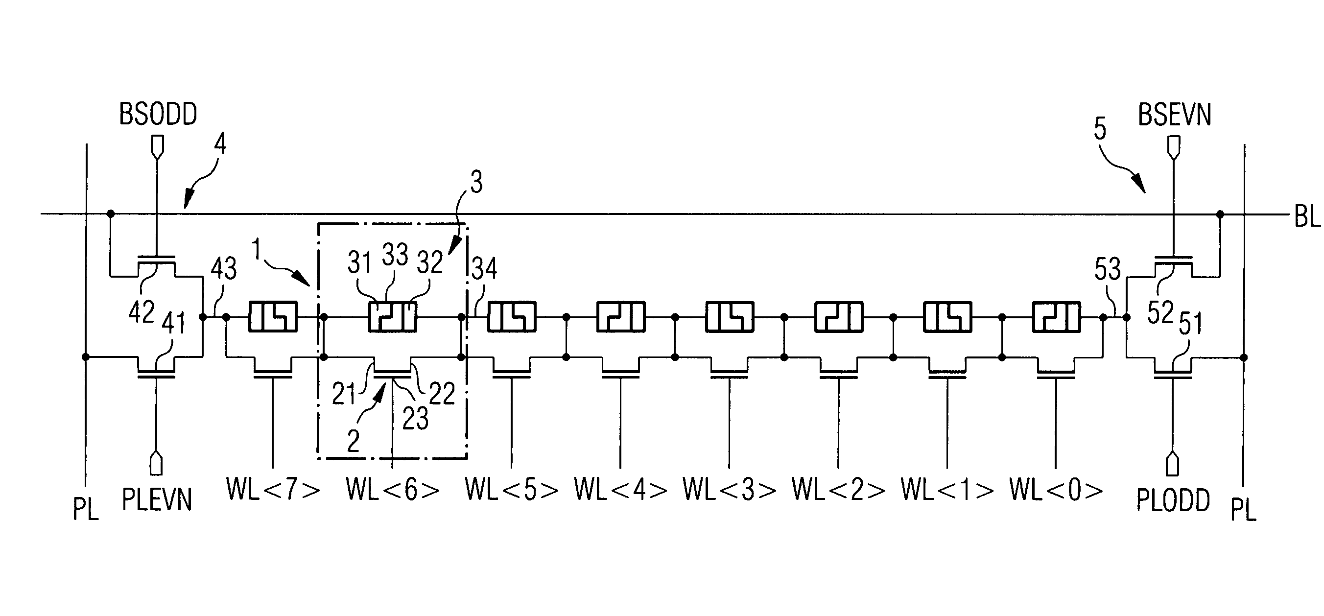
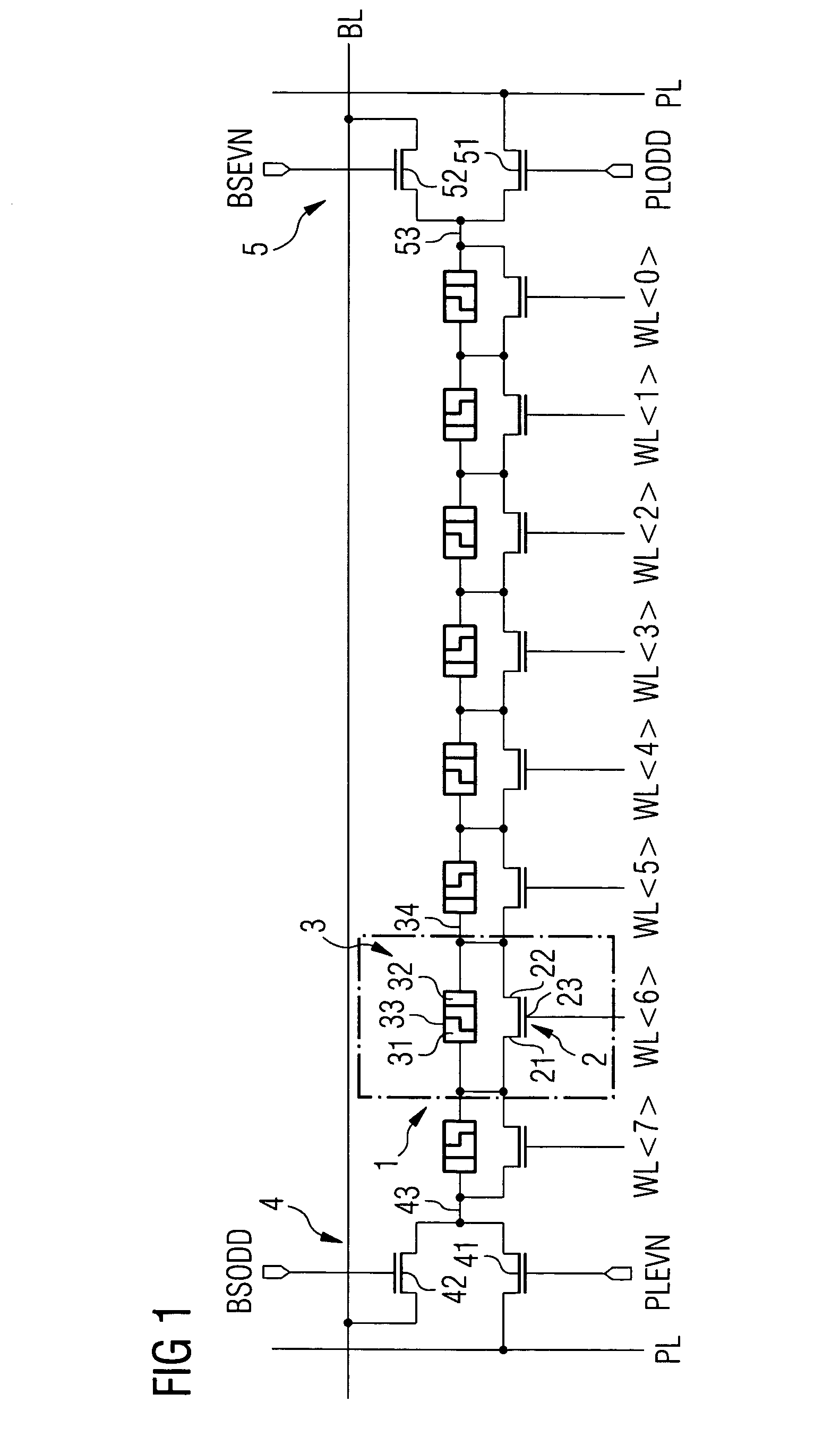
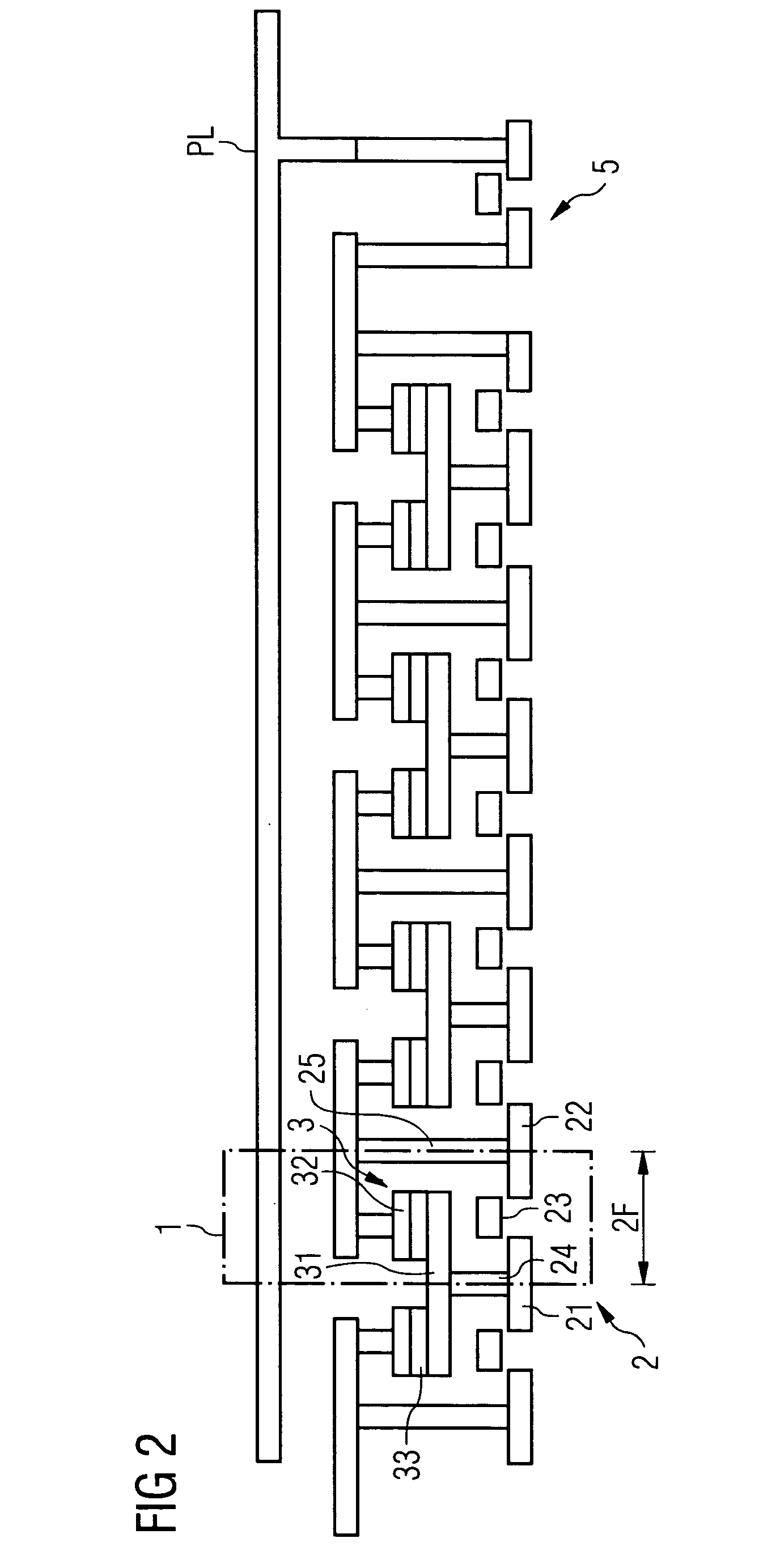
[0028]FIG. 1 schematically shows a detail from a memory circuit according to one embodiment of the invention with eight memory cells 1 connected in series between a ground line PL and a bit line BL. Each memory cell 1 has a drive transistor 2 and a resistance memory element 3, which are connected in parallel. As depicted, the resistance memory element 3 is composed of a cathode electrode 31, an anode electrode 32 and a storage layer 33 situated in between and is distinguished by a bipolar switching behavior. In other words, the polarity of the voltage applied between the electrodes of the resistance memory element 3 influences the activation operation of the resistance memory element 3.

[0029]In one embodiment, the bipolar resistance memory element 3 is a resistance memory element that is also known as a PMC (programmable metallization cell), where the anode electrode 32 is a reactive electrode and the cathode electrode 31 is an inert electrode, between which a porous, highly resisti...


PUM


Abstract

In a memory circuit having memory cells which are connected in series between a ground line PL and a bit line BL and in each case have a resistance memory element said element having a bipolar switching behavior having an anode electrode and a cathode electrode, and a drive transistor connected in parallel with the resistance memory element, the drive transistors of the memory cells in each case are connected to a word line in order to switch the drive transistor on and off in such a way that a current path is formed via the associated drive transistor in a non-activated state of a memory cell and a current path is formed via the associated resistance memory element in an activated state of a memory cell, a first changeover switch being arranged at one end and a second changeover switch at other ends of the series of memory cells in order alternately to produce a connection between the series-connected memory cells and the ground line and the bit line in a manner dependent on an applied address.

Description

CROSS-REFERENCE TO RELATED APPLICATIONS[0001]This application claims foreign priority benefits under 35 U.S.C. §119 to co-pending German patent application number DE 10 2004 041 330.4, filed 26 Aug. 2004. This related patent application is herein incorporated by reference in its entirety.BACKGROUND OF THE INVENTION[0002]1. Field of the Invention[0003]The invention relates to a memory circuit having memory cells which have a resistance memory element, wherein the resistance memory element exhibits a bipolar switching behavior.[0004]2. Description of the Related Art[0005]The development of semiconductor memory technology is essentially driven by the requirement for increasing the performance of the semiconductor memories in conjunction with miniaturization of the feature sizes. However, further miniaturization of the semiconductor memory concepts based on storage capacitors may be difficult due to the large quantity of charge that is required for writing to and reading from the storag...

Claims


Application Information

Patent Timeline
Patent Type & Authority Patents(United States)
IPC IPC(8): G11C17/00G11C11/00
CPCB82Y10/00G11C13/0011G11C13/0014G11C13/0016G11C13/003G11C13/0004G11C2213/75H10B63/30H10B63/80H10N70/24H10N70/231H10N70/245H10N70/20H10N70/8416H10N70/826H10N70/8822H10N70/8825H10N70/8828H10N70/8836
Inventor ROEHR, THOMAS
Owner POLARIS INNOVATIONS LTD
Why Eureka
Try Eureka