
Device with integrated capacitance structure

a capacitance structure and integrated technology, applied in semiconductor devices, semiconductor/solid-state device details, capacitors, etc., can solve the problems of defective contact-connection, different structure dimensions of metal dots and lattice frames, disadvantages in design, layout and production engineering, etc., to achieve the maximum utilization of vertical capacitance portions, ensure the effect of high yield and low thermomechanical loading

Active Publication Date: 2007-05-29
INFINEON TECH AG
View PDF5 Cites 3 Cited by
  • Summary
  • Abstract
  • Description
  • Claims
  • Application Information

AI Technical Summary

Benefits of technology

The present invention provides a device with a capacitance structure that requires a maximum capacitance value and a minimum volume requirement. The device can be fabricated with high production quality and yield, and can be easily adapted to existing circuit arrangements. The capacitance structure includes two partial structures that are patterned above a substrate, which are enclosed by an insulation layer. The distance between the two partial structures is minimized to achieve a high capacitance value and a small lateral area requirement. The capacitance structure can be fabricated using existing tools for layout and design creation. The device can be used in various semiconductor components and can provide optimal properties for other active or passive circuit elements.

Problems solved by technology

The greatly different structure dimensions of metal dots and lattice frames are disadvantageous in terms of design, layout and production engineering.
Since the connecting elements (vias) proceed from crossover points of the lattice structure, a comparatively small lateral misalignment may result in defective contact-connection.
Known capacitance structures of this type can be integrated only with difficulty in existing standard cell libraries.

Method used


Image

  • Device with integrated capacitance structure
  • Device with integrated capacitance structure
  • Device with integrated capacitance structure

Examples


Embodiment Construction

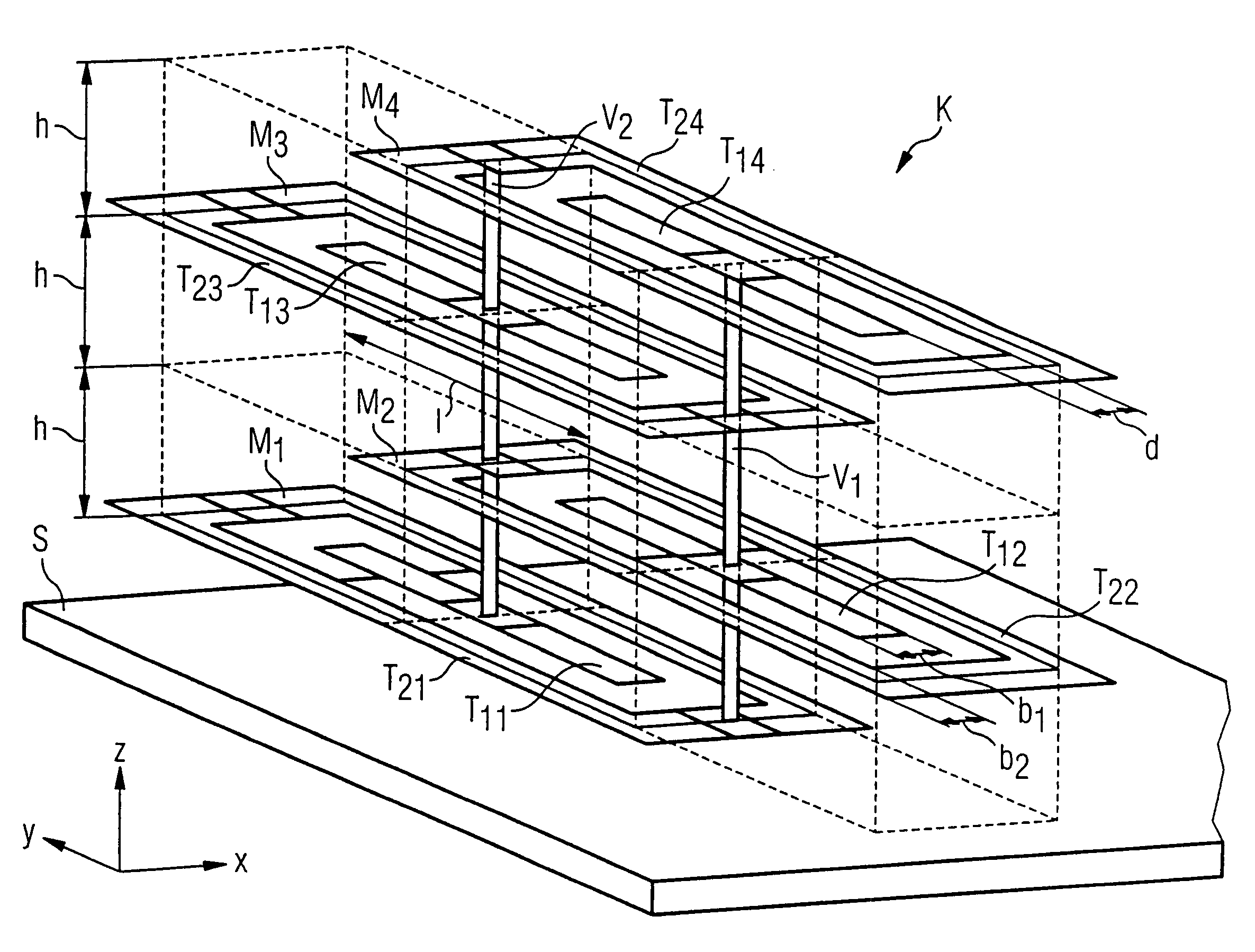
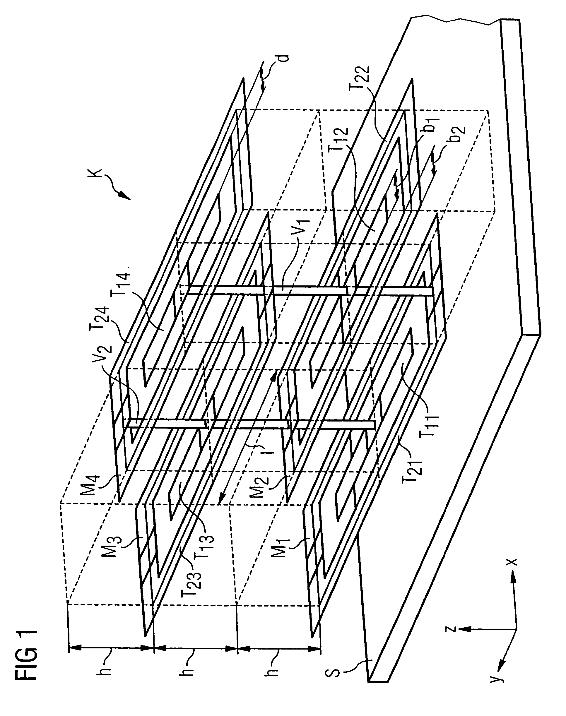
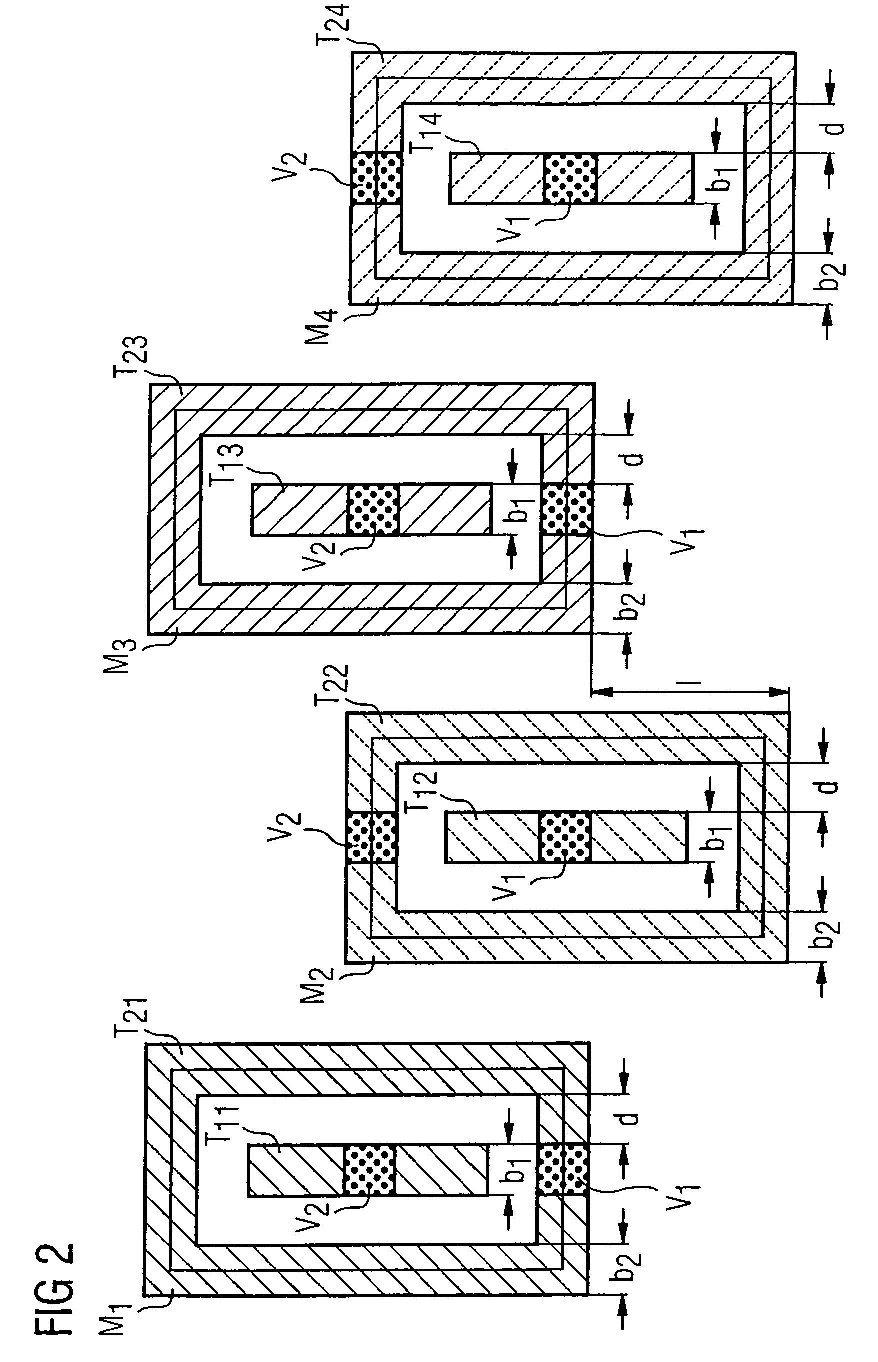
[0025]In FIG. 1, a semiconductor device has a capacitance arrangement or structure K embedded in an insulation layer or a system of insulation layers (not illustrated). The insulation layer used may be a layer or a layer sequence comprising silicon dioxide (SiO2), silicon nitride (Si3N4) or some other suitable insulating material. The insulation layer and the capacitance structure K are situated above a substrate S made, for example, of silicon (Si) or silicon carbide (SiC). An integrated circuit or a semiconductor component may be realized in the semiconductor substrate, so that the device is formed by this and the capacitance structure K. The substrate S may also be formed by a printed circuit or the like.

[0026]A first rewiring plane M1 is patterned in such a way that a first partial structure T11 is enclosed by a second partial structure T21. The distance between the two partial structures should preferably not exceed 250 nm in order to ensure optimum utilization of area. The par...


PUM


Abstract

The present invention relates to a device with integrated capacitance structure has at least one first and an adjacent second rewiring plane, each of which comprises at least one first partial structure and a second partial structure, which is different from the first partial structure, the second partial structure in each case substantially surrounding the first partial structure, and the first partial structure of the first rewiring plane being electrically connected to the second partial structure of the second rewiring plane and the second partial structure of the first rewiring plane being electrically connected to the first partial structure of the second rewiring plane and forming different poles of the capacitance structure.

Description

CLAIM FOR PRIORITY[0001]This application claims the benefit of priority to German Application No. 10 2004 047 660.8 which was filed in the German language on Sep. 30, 2004,the contents of which are hereby incorporated by reference.TECHNICAL FIELD OF THE INVENTION[0002]The present invention relates to a device with integrated capacitance structure.BACKGROUND OF THE INVENTION[0003]In semiconductor technology, for the integration of analogue circuit elements, there is a need for passive components, in particular capacitances, of high production quality and reproducibility in conjunction with a large capacitance value and a small area requirement. Since the advancing large-scale integration of semiconductor components means that the lateral dimensions are decreasing to a greater extent in relation to the vertical dimension, the lateral portions of capacitance structures are increasingly gaining in importance.[0004]In the case of a capacitance structure disclosed in U.S. Pat. No. 6,411,4...

Claims


Application Information

Patent Timeline
Patent Type & Authority Patents(United States)
IPC IPC(8): H01L21/8242H10B12/00
CPCH01L23/5223H01L28/87H01L2924/0002H01L2924/00
Inventor KROPF, CLAUS
Owner INFINEON TECH AG
Learn More