
Eureka
For R&D, Eureka makes reading and utilizing patents & technical documents easy.
Eureka AIR
Designed for self-driven R&D workflows. Generate viable solutions, solve complex R&D challenges, empower your innovation with AI.

Eureka Materials
Designed for material experts only. Revolutionize your material R&D, from search, analyze, to developing new materials.

TechResearch
Generate reliable direction feasibility study reports for your R&D in just a few steps.

TechSeek
Discover and master advanced knowledge NOW. Basics, ideas, possibilities, all at once.

TechMind
As an expert in R&D Theories, TechMind can generates customized viable solutions instantly.

TechRisk
Analyze your overall solution with one click, know your potential R&D risks in advance.

TechMonitor
Get weekly tech updates, stay abreast of the latest tech innovations and key insights.
Method of manufacturing a semiconductor device that includes implanting in multiple directions a high concentration region
- Summary
- Abstract
- Description
- Claims
- Application Information
AI Technical Summary
Benefits of technology
Problems solved by technology
Method used
Image

Examples
first embodiment
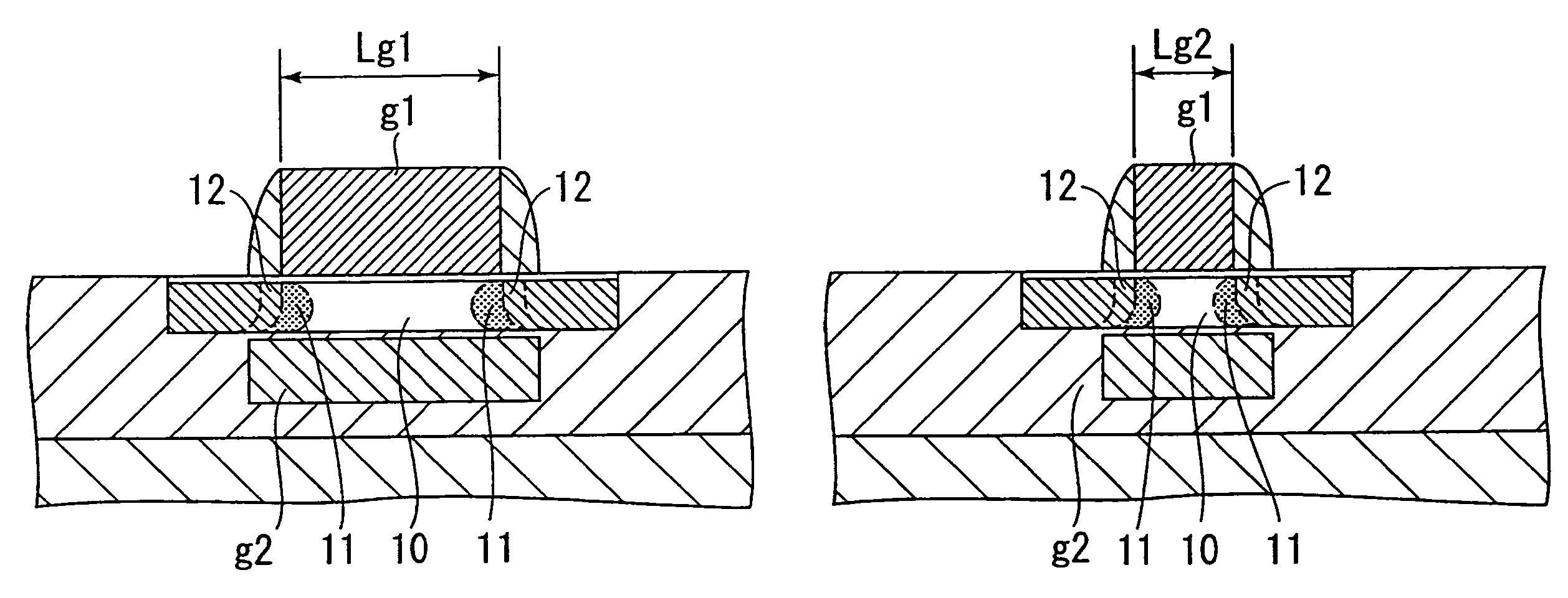
[0034]Hereinafter, embodiments of the present invention are described on the basis of the attached drawings. FIG. 1 is a schematic section diagram illustrating a semiconductor device according to a The semiconductor device 1 is composed of a complete depletion type SOI transistor formed on an SOI layer 23 formed on an SIMOX substrate 20 (or a low dose SIMOX).
[0035]In the SOI film 23, there are a channel formation portion 10 formed at the central portion thereof, a source 4 and a drain 5 formed on both the end parts thereof. In addition, a gate 2 is formed above the channel formation portion 10 with an insulation film 2a put between them.
[0036]Side walls 3 are formed on both the sides of the gate 2 and extension regions 12 are formed in the SOI film located below the side walls 3.
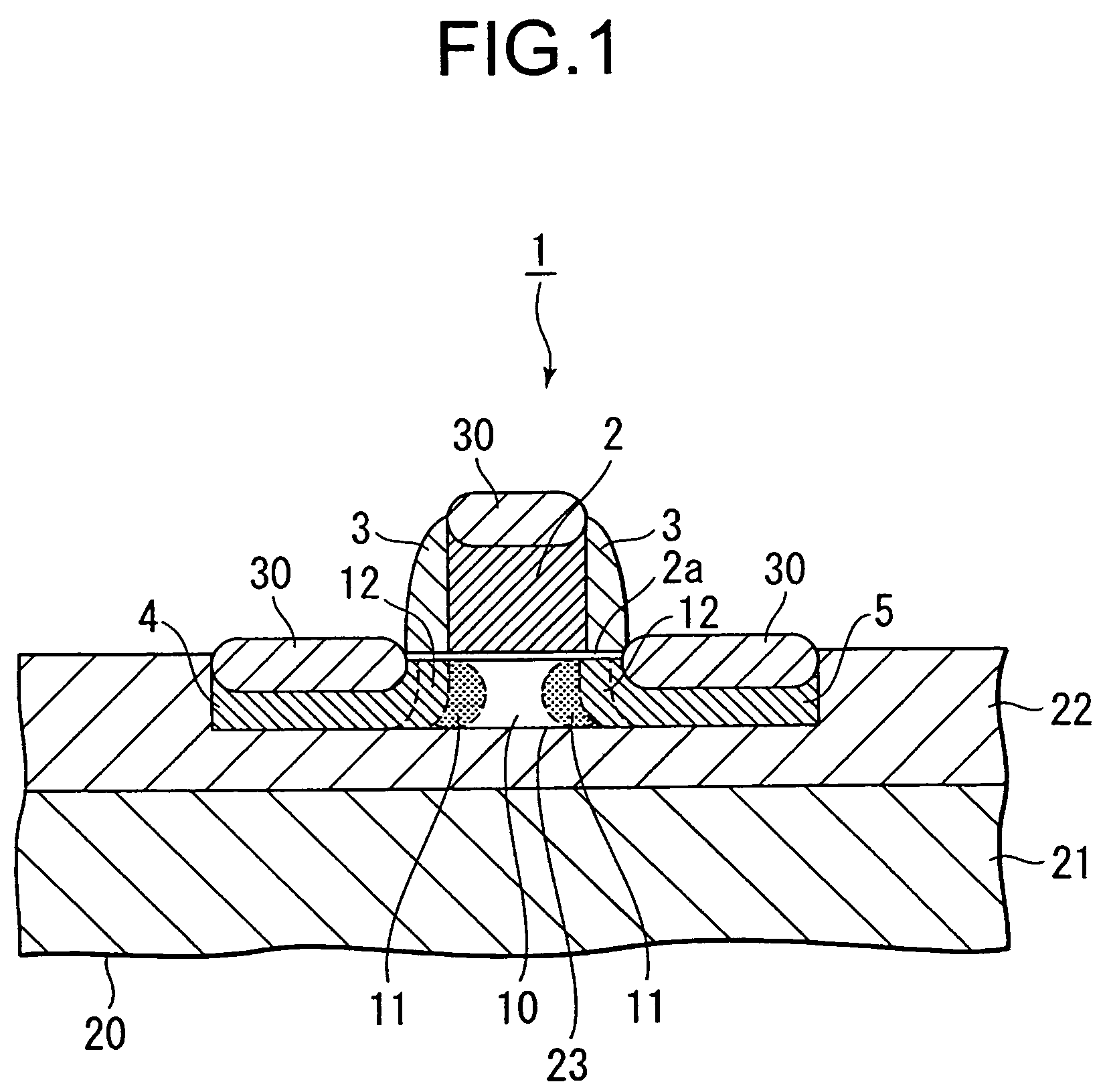
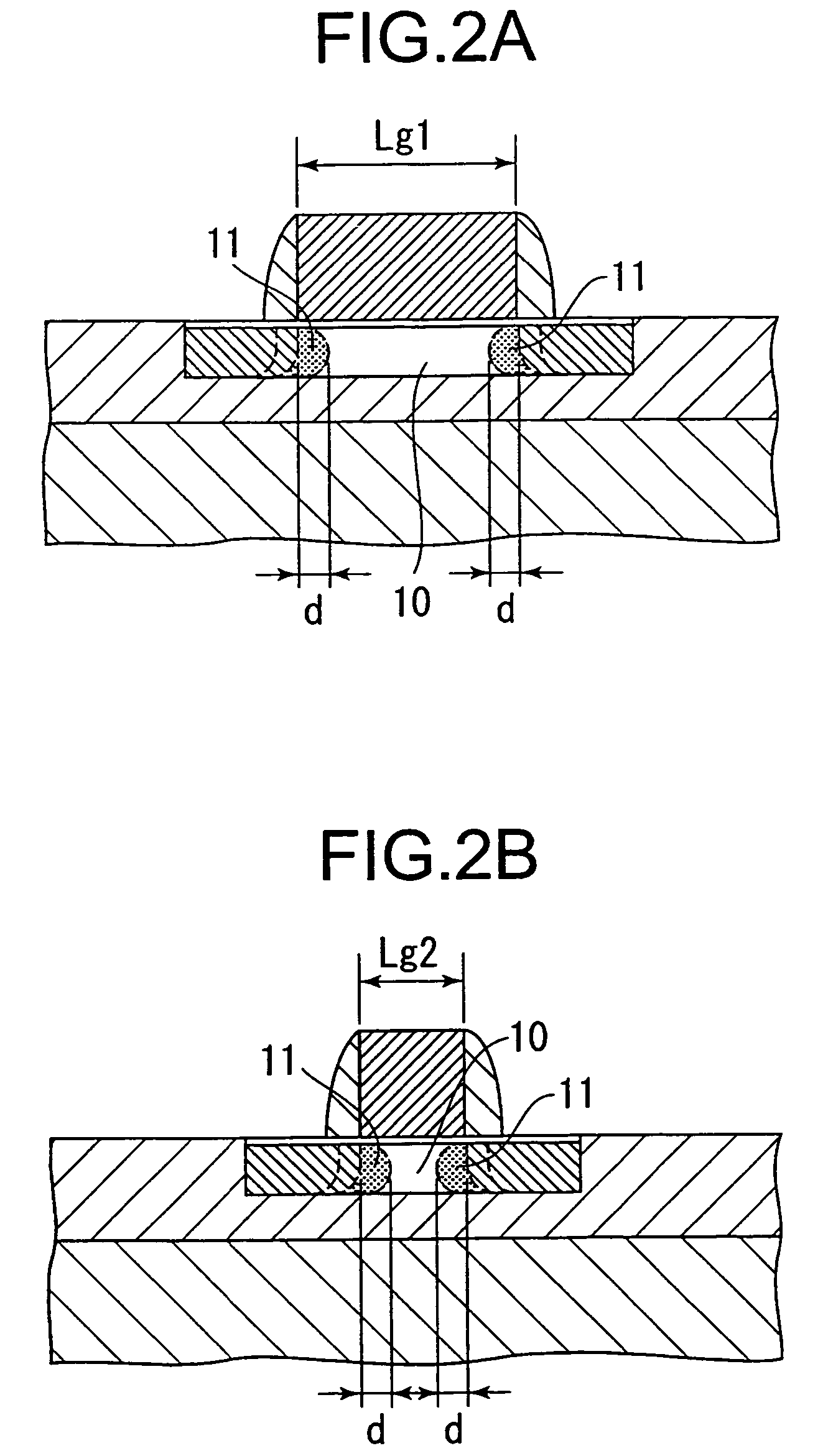
[0037]In such a complete depletion type SOI transistor, the present embodiment is characterized in that impurity concentrations in the channel formation portion 10 are implanted not uniformly along the leng...
second embodiment
[0110]By such a semiconductor device it becomes possible to suppress the dependency of a threshold value on the thickness of the SOI film in a complete depletion type SOI transistor even though the threshold value is controlled by means of the impurity concentration of the channel formation portion. As a result, the dependency of the threshold value to the thickness of the SOI film is eased so as to make it possible to increase the uniformity of the threshold value and to improve the characteristics of making the electrical power consumption lower (electrical power consumption lowering characteristics).
[0111]It is to be noted that the contents described above are only an example of the present invention, and the present invention is not restricted to the value of each of such process conditions. In addition, any substrate on the market made by lamination methods such as ELTRAN, Unibond and the like can be used as an SOI substrate besides the SIMOX substrate. Furthermore, although a...
third embodiment
[0125]Next, a method of manufacturing of the semiconductor device is described. FIGS. 12A-12C, 13A-13C and 14A-14C are diagrams illustrating the method of manufacturing of the semiconductor device according to the present embodiment. At first, a back surface gate g2 is formed in the inside of a substrate while a laminated SOI substrate 20a is made, by a well-known technique disclosed in IEDM '91 pp. 683 (Tetsu Tanaka, et al.) or Japanese Patent Laid-Open Publication No. Hei 10-125881. In the case where the SOI substrate is worked by these techniques, after selection grinding using a stopper, the SOI substrate is in the state in which an active region of a MOS FET is patterned (element isolation) (see FIG. 12A).
[0126]Now, the back surface gate g2 is composed of p+ poly Si of 150 nm in which, for example, B+ is sufficiently doped. The thickness of an insulation film 2b being a back surface gate oxide film is, for example, 30 nm.
[0127]Next, as shown in FIG. 12B, after SiO2 is grown on...
PUM
 Abstract
Description
Claims
Application Information
 - R&D Engineer
- R&D Manager
- IP Professional
- Industry Leading Data Capabilities
- Powerful AI technology
- Patent DNA Extraction
Browse by: Latest US Patents, China's latest patents, Technical Efficacy Thesaurus, Application Domain, Technology Topic, Popular Technical Reports.
© 2024 PatSnap. All rights reserved.Legal|Privacy policy|Modern Slavery Act Transparency Statement|Sitemap|About US| Contact US: help@patsnap.com