Current sensor having hall element

a technology of current sensor and hall element, which is applied in the direction of instruments, magnetic measurements, and measurement using dc-ac conversion, etc., can solve the problems of restricted positioning between the hall element and the current path, and achieve the reduction of the dimension of the sensor, the prevention of detection accuracy of the sensor, and the effect of high detection accuracy

Inactive Publication Date: 2007-08-07
DENSO CORP
View PDF10 Cites 11 Cited by
  • Summary
  • Abstract
  • Description
  • Claims
  • Application Information

AI Technical Summary

Benefits of technology

[0007]In view of the above-described problem, it is an object of the present disclosure to provide a current sensor having small dimensions and high detection accuracy.
[0009]In the above sensor, the Hall element is a vertical type Hall element, and the sensor can detect the detection object current without a magnetic field concentration member. Thus, the dimensions of the sensor are minimized. Further, the positioning between the Hall element and the current path is much accurately determined. Thus, deviation of the positioning between the Hall element and the current path is restricted. Thus, the detection accuracy of the sensor is prevented from deviating. Accordingly, the sensor has small dimensions and high detection accuracy.

Problems solved by technology

Thus, deviation of the positioning between the Hall element and the current path is restricted.

Method used


Image

  • Current sensor having hall element
  • Current sensor having hall element
  • Current sensor having hall element

Examples


first embodiment

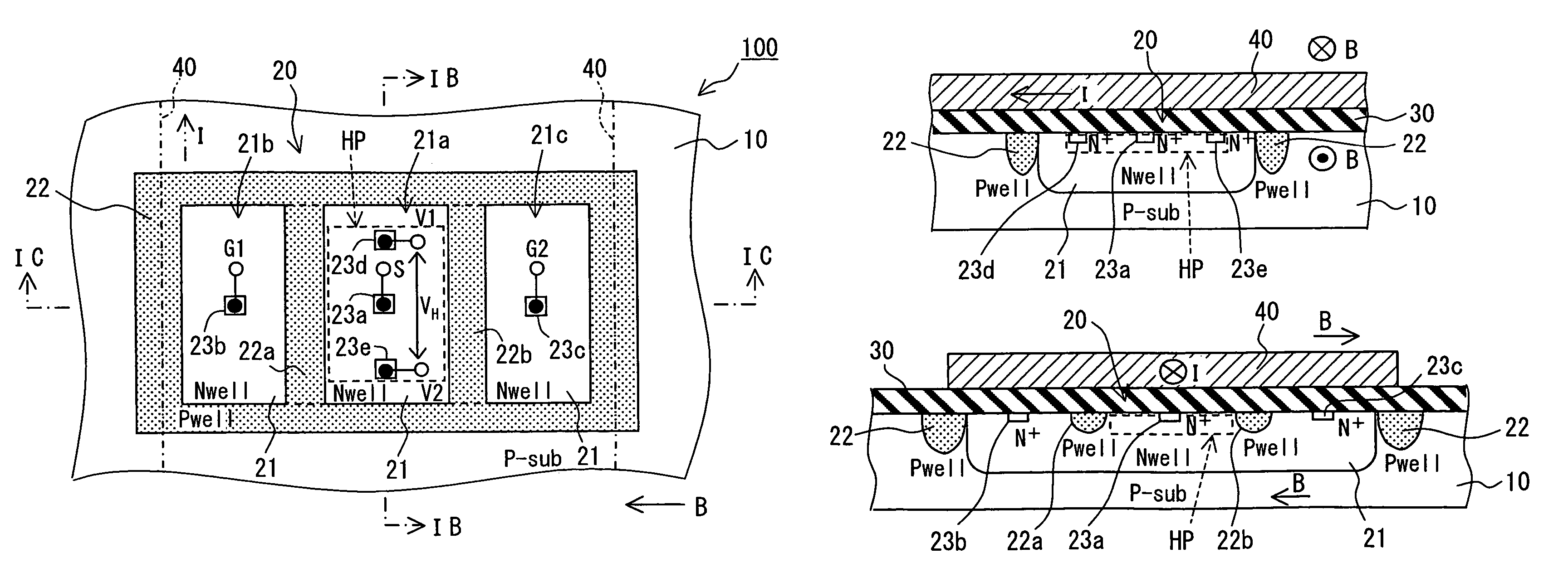
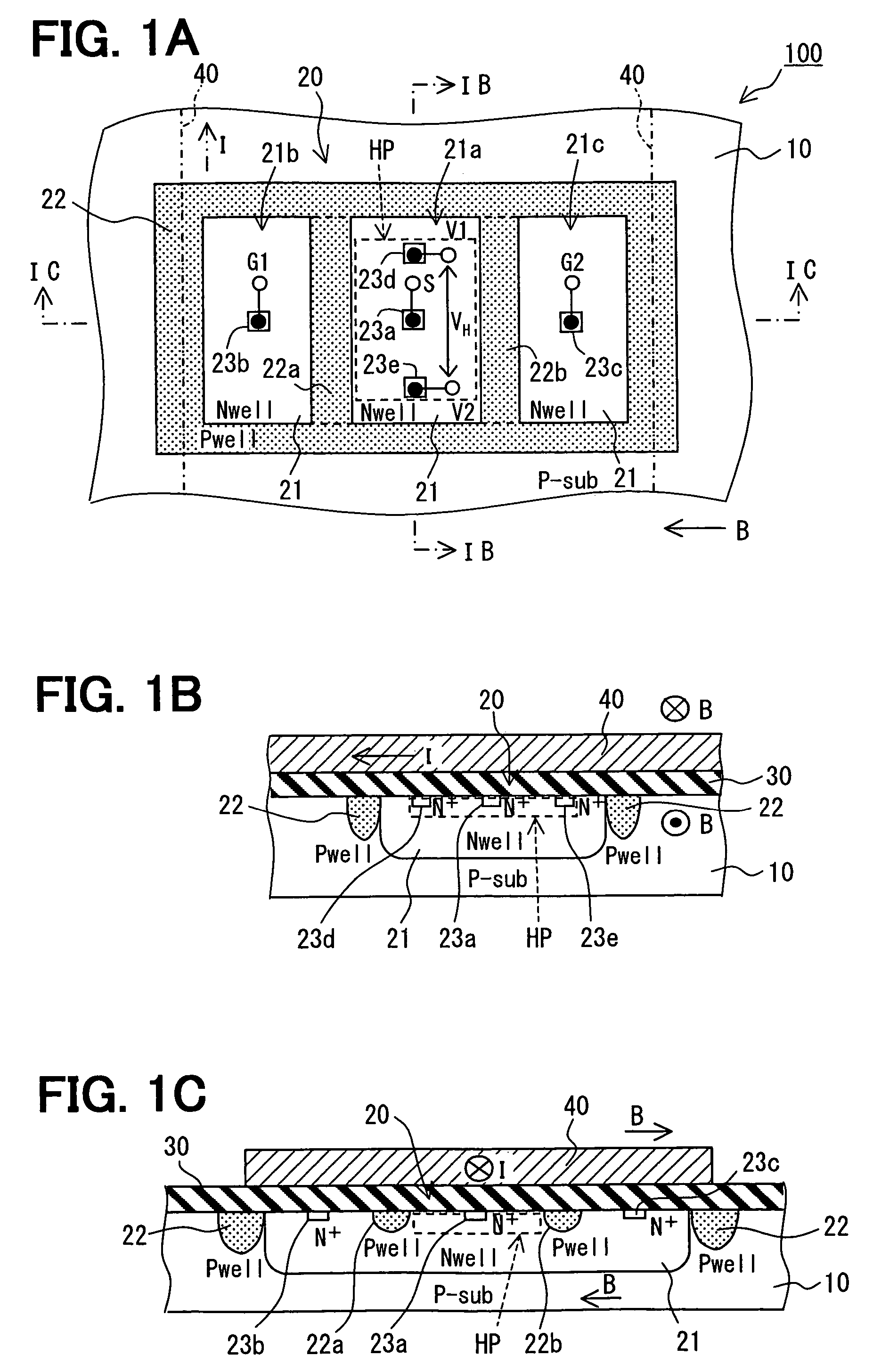
[0016]A current sensor 100 according to a first embodiment of the present invention is shown in FIGS. 1A to 1C. Here, in FIG. 1, an insulation layer 30 is not shown, and a wiring portion 40 surrounded with two dotted lines is transparently shown.

[0017]The current sensor 100 includes a semiconductor substrate 10, a Hall element 20 and a wiring portion 40. The Hall element 20 is formed on one side of the substrate 10. The wiring portion 40 is formed on the one side of the substrate 10 through the insulation layer 30. Here, the constitution of the Hall element and the manufacturing method of the hall element are described in US 2005 / 0,230,770-A1.

[0018]In the sensor 100, the substrate 10 is made of a silicon substrate (i.e., P-sub) having a P conductive type. Specifically, the substrate has a (100)-crystal orientation surface as a cutting surface. By using the P-sub, an offset voltage caused by stress applied to the substrate 10 is reduced. Alternatively, the substrate 10 may be made of...

second embodiment

[0035]A current sensor 200 according to a second embodiment of the present invention is shown in FIG. 4. In FIG. 4, the insulation layer 30 is not shown on the substrate 10. Further, the wiring portion 40 on the insulation layer 30 is transparently shown.

[0036]The sensor 200 includes not only the Hall element 20 but also a processing circuit portion 50. The Hall element 20 and the processing circuit portion 50 are integrally formed on the same substrate 10. The processing circuit portion 50 includes a signal processing circuit and a current driving circuit. The signal processing circuit calculates the Hall voltage signal outputted from the Hall element 20, and the current driving circuit controls and supplies the driving current to the Hall element 20.

[0037]In this case, since the processing circuit portion 50 is integrated into the same substrate 10, in which the Hall element 20 is formed, the total dimensions of the sensor 200 become much smaller.

third embodiment

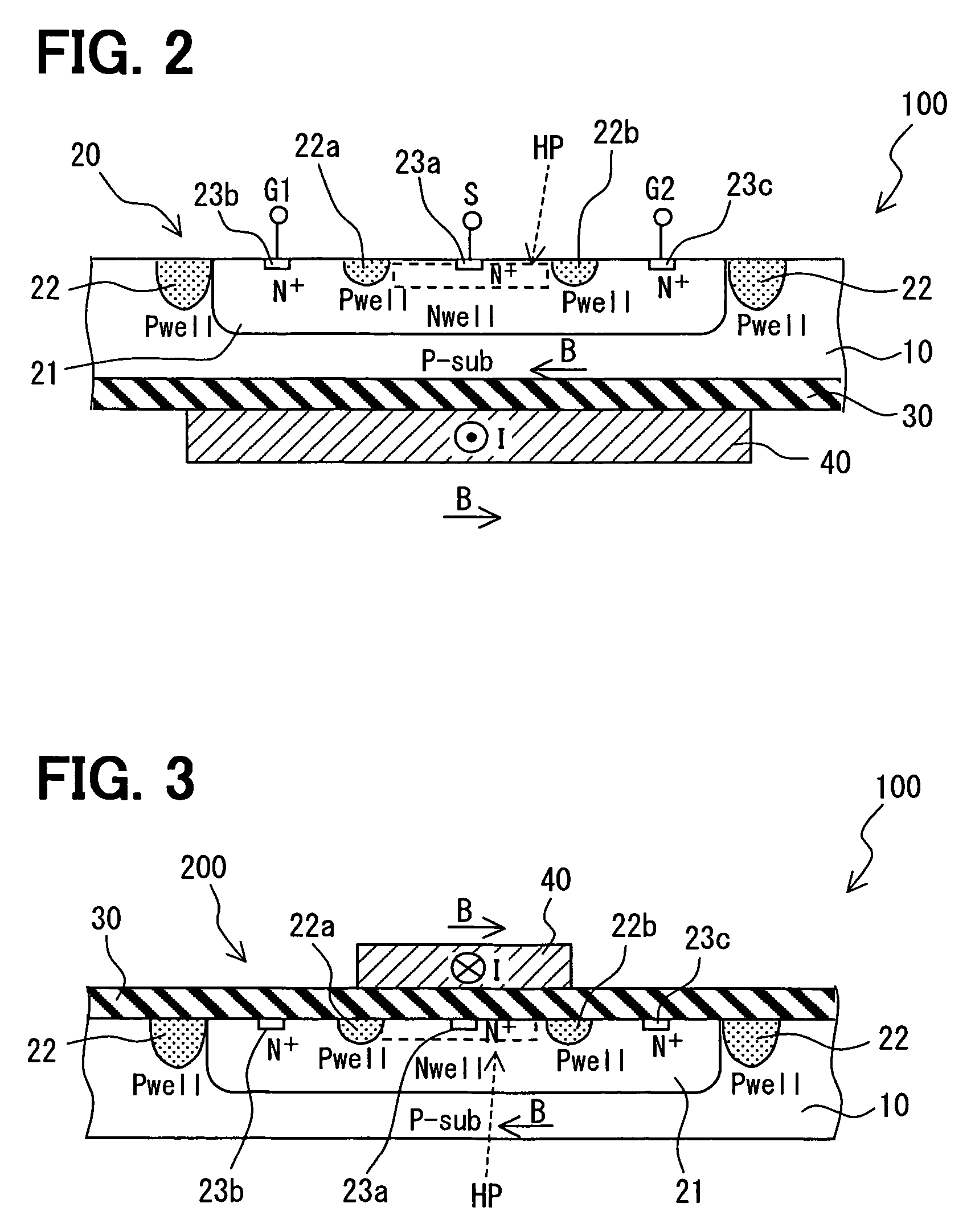
[0038]A current sensor 300 according to a third embodiment of the present invention is shown in FIG. 5. The sensor 300 includes a wiring portion 41 as a current path. The wiring portion 41 is disposed over the substrate 10 through an insulation member 31. Specifically, the insulation member 31 has a frame shape, and is made of insulation material such as resin. The insulation member 31 is bonded to and fixed on the surface of the substrate 10. The wiring member 41 is bonded to an opposite side of the insulation member 31, the opposite side which is opposite to the substrate 10. The wiring member 41 is formed from a metallic plate such as a copper plate. The metallic plate is processed to be a predetermined shape so that the wiring member 41 is formed.

[0039]In this case, the wiring member 41 is integrally formed on the semiconductor substrate 10 through the insulation member 31 without using the semiconductor process.

[0040]The present disclosure has the following aspects.

[0041]Accord...


PUM


Abstract

A current sensor includes: a current path; a semiconductor substrate; and a Hall element on the substrate. The Hall element detects a magnetic flux in a magnetic field caused by a detection object current. The Hall element generates a Hall voltage corresponding to the magnetic flux when a driving current flowing in a direction perpendicular to the semiconductor substrate is supplied to the Hall element, and when the magnetic flux having a component parallel to the semiconductor substrate affects the Hall element. The current path is disposed on the semiconductor substrate. The current path is electrically isolated from the Hall element.

Description

CROSS REFERENCE TO RELATED APPLICATION[0001]This application is based on Japanese Patent Application No. 2005-181091 filed on Jun. 21, 2005, the disclosure of which is incorporated herein by reference.FIELD OF THE INVENTION[0002]The present invention relates to a current sensor having a Hall element.BACKGROUND OF THE INVENTION[0003]Conventionally, a current sensor having a lateral type Hall element for detecting current flowing through a current path is well known. The lateral type Hall element is formed on a semiconductor substrate, and the Hall element detects a magnetic flux in a vertical direction of the substrate. The current sensor detects the magnetic flux by using the Hall element in a case where the magnetic flux is generated in a magnetic field when the current as a detecting object flowing though the current path. In the current sensor, the current path passes through a magnetic field concentration core having a C-shape, and a sensor chip including the Hall element is mou...

Claims


Application Information

Patent Timeline
Patent Type & Authority Patents(United States)
IPC IPC(8): G01R15/20
CPCG01R15/202
Inventor ISHIO, SEIICHIRO
Owner DENSO CORP
Why Eureka
Try Eureka