Waveguide device and method for making same

a waveguide and micromachine technology, applied in waveguides, instruments, photomechanical equipment, etc., can solve the problems of increasing mass and cost, time-consuming and labor-intensive labor, and traditional fabrication techniques cannot easily fabricate small high-frequency waveguides. , the effect of increasing the mass and cos

Active Publication Date: 2007-08-14
SANDIA NAT LAB
View PDF3 Cites 6 Cited by
  • Summary
  • Abstract
  • Description
  • Claims
  • Application Information

AI Technical Summary

Benefits of technology

[0008]The present invention relates to monolithic micromachined waveguide for the transmission of energy within or near the microwave region of the electromagnetic spectrum, and a method of manufacturing the same. The waveguide of the present invention includes the capability to be formed with high-aspect ratios including channels with heights of many hundreds of microns (or up to approximately 3 mm) and lateral widths of much less than a single micron (or approximately 0.2 microns), and the ability to transmit frequencies between 1 and 300 GHz with the greatest benefit realized at higher frequencies.

Problems solved by technology

The manufacture of conventional waveguides is a time, labor, and capital-intensive undertaking, involving either Computerized Numerical Control (“CNC”) milling, turning and drilling or electroplating over existing molds.
Further, traditional fabrication techniques cannot easily fabricate smaller high-quality, high-frequency waveguides.
The biggest disadvantage of conventionally fabricated waveguide components is that they must be individually fabricated and later assembled, leading to increased mass and cost.
Further, there are limits to how small a conventionally fabricated waveguide can be made, limiting the frequency range of this particular type of waveguide.

Method used


Image

  • Waveguide device and method for making same
  • Waveguide device and method for making same
  • Waveguide device and method for making same

Examples


Embodiment Construction

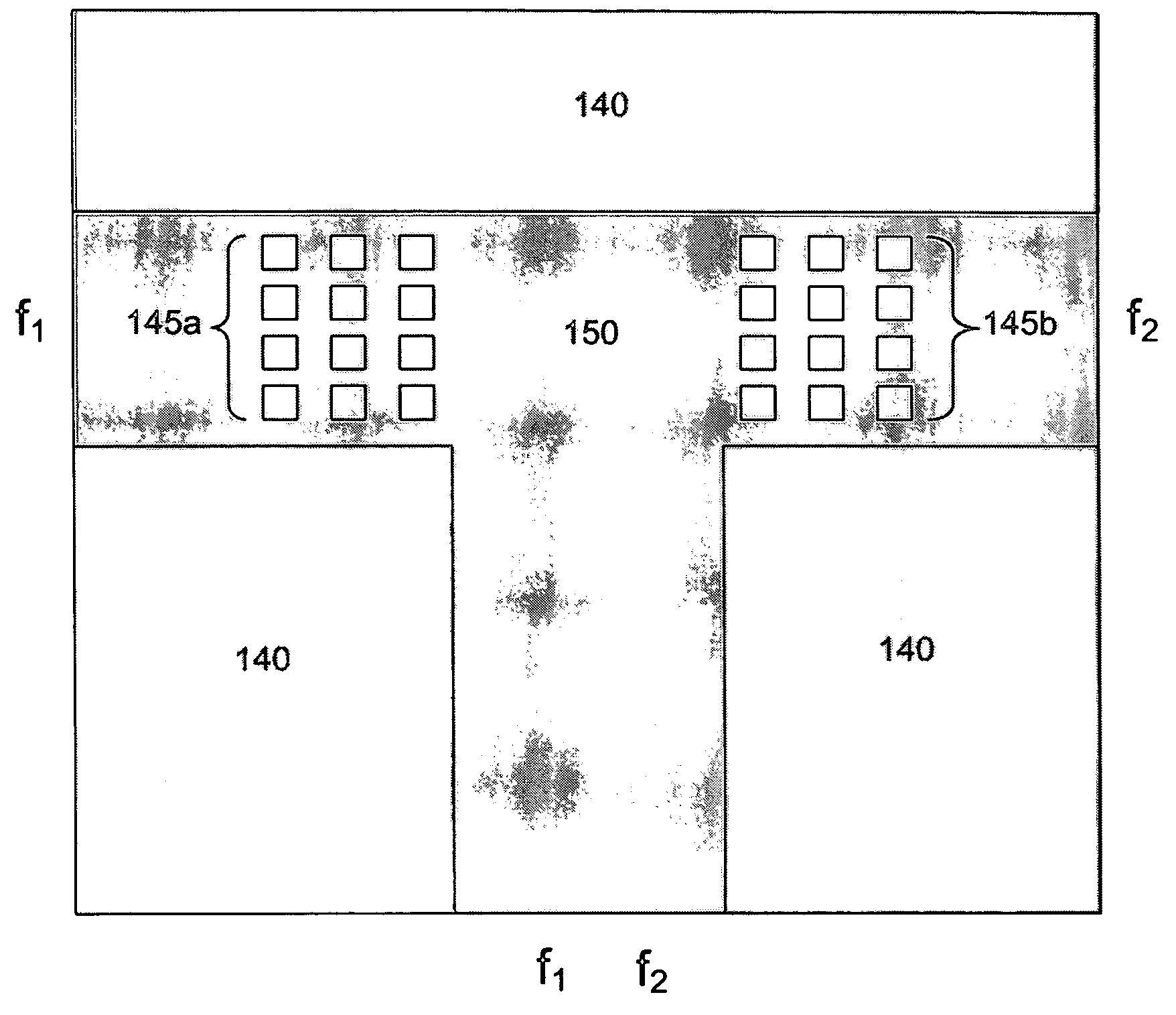
[0018]The following description of illustrative, non-limiting embodiments of the invention discloses specific configurations and components. However, the embodiments are merely examples of the present invention, and thus, the specific features described below are merely used to describe such embodiments to provide an overall understanding of the present invention. One skilled in the art readily recognizes that the present invention is not limited to the specific embodiments described below. Furthermore, certain descriptions of various configurations and components of the present invention that are known to one skilled in the art are omitted for the sake of clarity and brevity.

[0019]An embodiment of the present invention utilizes a manufacturing process known as “LIGA” (an acronym derived from the German “Lithographie, Galvanoformung, and Abformung”). The main steps of the LIGA process are deep x-ray lithography, electroforming, and plastic molding. The LIGA process has typically bee...


PUM

PropertyMeasurementUnit
rms roughnessaaaaaaaaaa
angleaaaaaaaaaa
angleaaaaaaaaaa

Abstract

A monolithic micromachined waveguide device or devices with low-loss, high-power handling, and near-optical frequency ranges is set forth. The waveguide and integrated devices are capable of transmitting near-optical frequencies due to optical-quality sidewall roughness. The device or devices are fabricated in parallel, may be mass produced using a LIGA manufacturing process, and may include a passive component such as a diplexer and/or an active capping layer capable of particularized signal processing of the waveforms propagated by the waveguide.

Description

STATEMENT OF GOVERNMENT SUPPORT[0001]The United States Government has rights in this invention pursuant to Contract No. DE-AC04-94AL85000 between the United States Department of Energy and Sandia Corporation for the operation of Sandia National Laboratories.CROSS-REFERENCE TO RELATED APPLICATIONS[0002]This application incorporates by reference the patent application entitled Micromachined Microwave Signal Control Device and Method for Making Same, with Ser. No. 11 / 149,400, filed on the same day as the present application.FIELD OF THE INVENTION[0003]The present invention relates to monolithic micromachined waveguides for the transmission of microwave signals, and a method for making the same. The device may include integrated passive components such as a diplexer and / or an active component layer.BACKGROUND OF THE INVENTION[0004]Waveguides are critical components for radar and communications systems, and are often used in conjunction with switches, couplers, splitters, filters, and ot...

Claims


Application Information

Patent Timeline
Patent Type & Authority Patents(United States)
IPC IPC(8): H01P3/00G02B6/10G02B6/136G03C5/00H01P5/12
CPCG02B6/102G02B6/1221G02B6/136G03F7/0005H01P1/2005H01P3/12H01P11/002
Inventor FORMAN, MICHAEL A.
Owner SANDIA NAT LAB
Why Eureka
Try Eureka