
Image forming method, image forming apparatus, optical scan device, and image forming apparatus using the same

a technology of image forming apparatus and pattern reading, applied in the field of image forming method optical scan device, image forming apparatus using the same, can solve the problems of incorrectly performed, inability to obtain a high-quality image, and considerable errors in reading pattern for detecting variation in registration

Inactive Publication Date: 2007-08-14
RICOH KK
View PDF49 Cites 58 Cited by
  • Summary
  • Abstract
  • Description
  • Claims
  • Application Information

AI Technical Summary

Benefits of technology

[0028]Accordingly, it is a general object of the present invention to provide an improved and useful image forming method, tandem laser scan optical device, optical scan device, and image forming apparatus using the optical scan device in which the above-mentioned problems are eliminated.
[0029]It is another and more specific object of the present invention to provide a tandem laser scan optical device that saves energy and corrects print position shift of main scan caused by variation in temperature and the like.
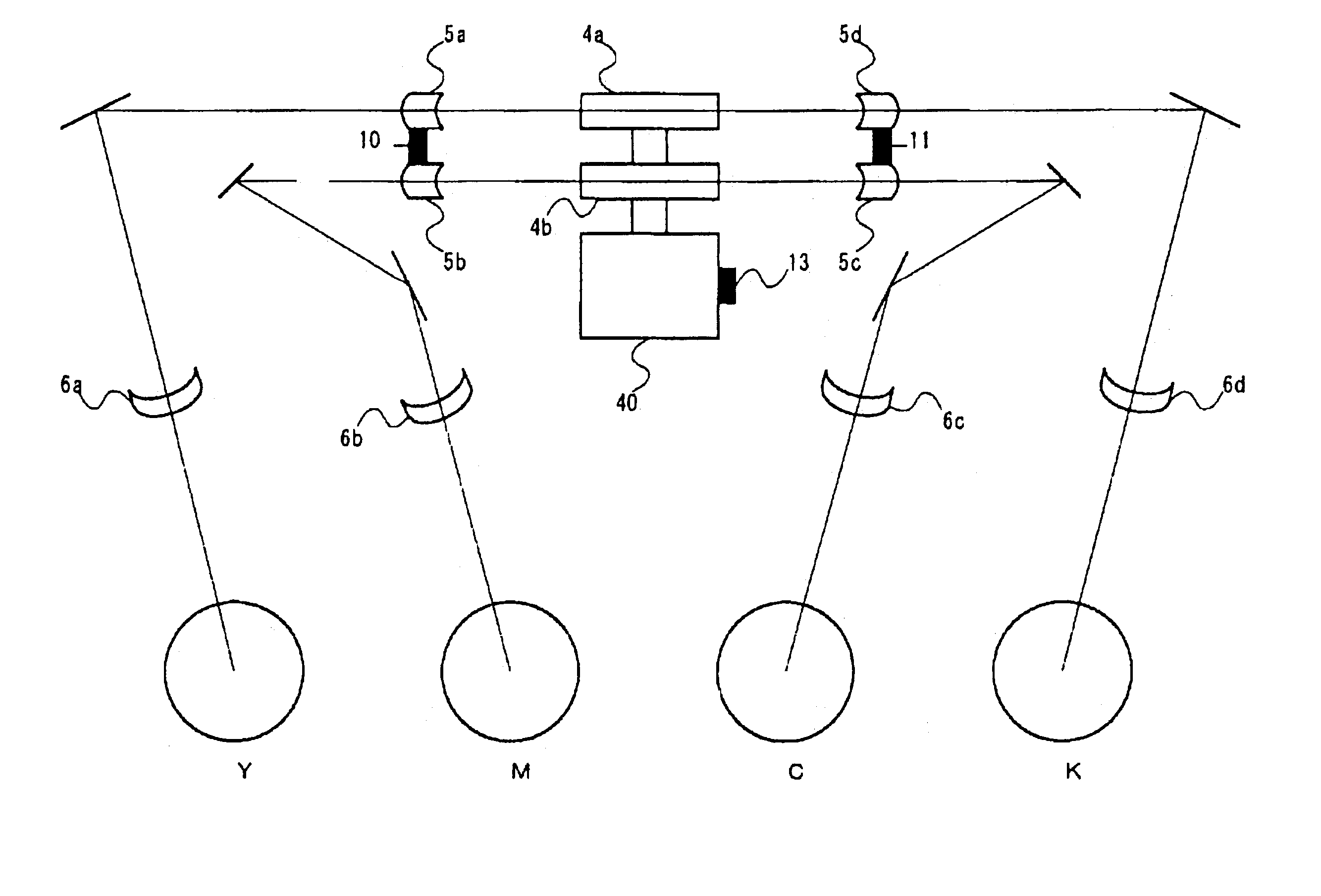
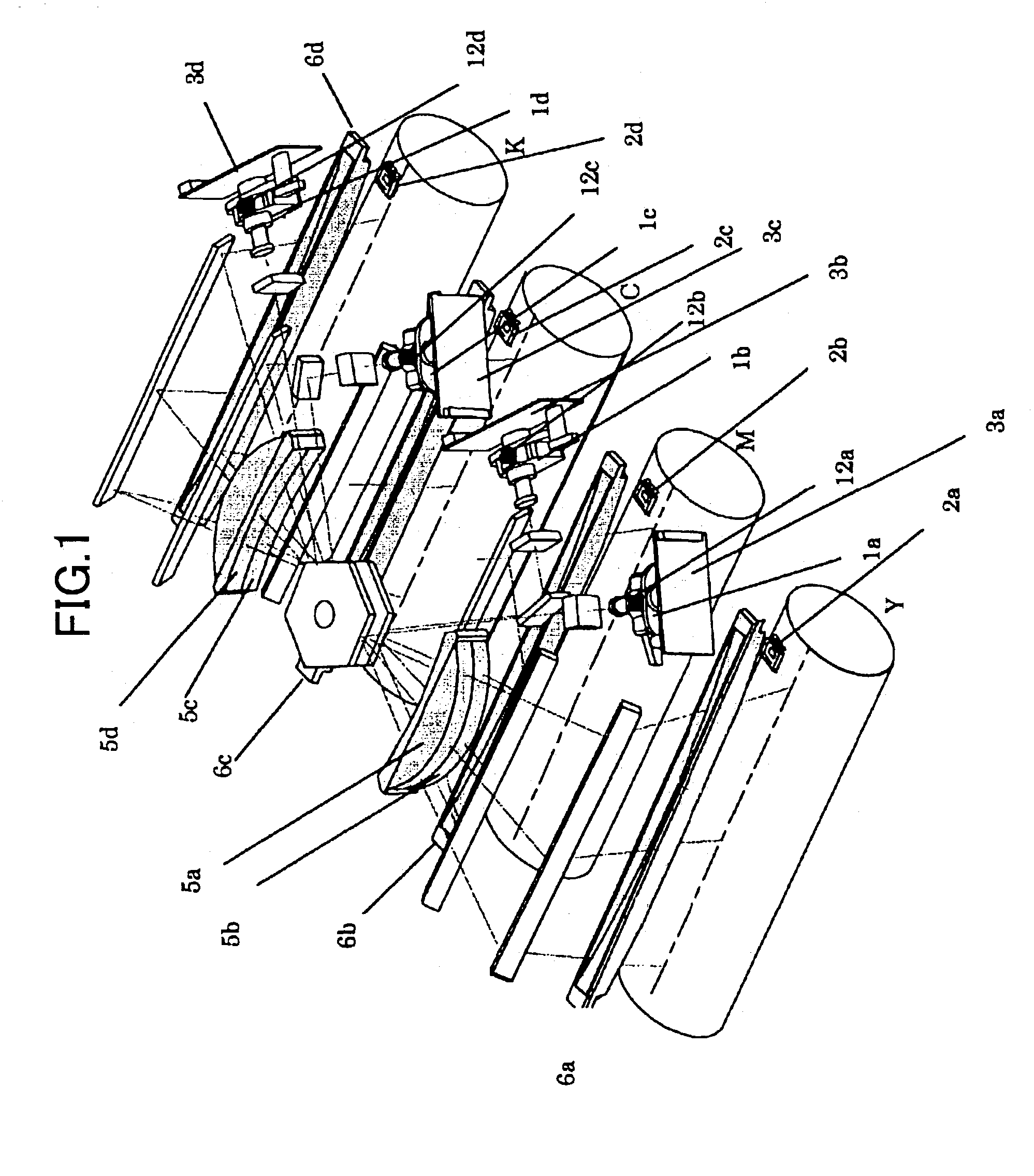
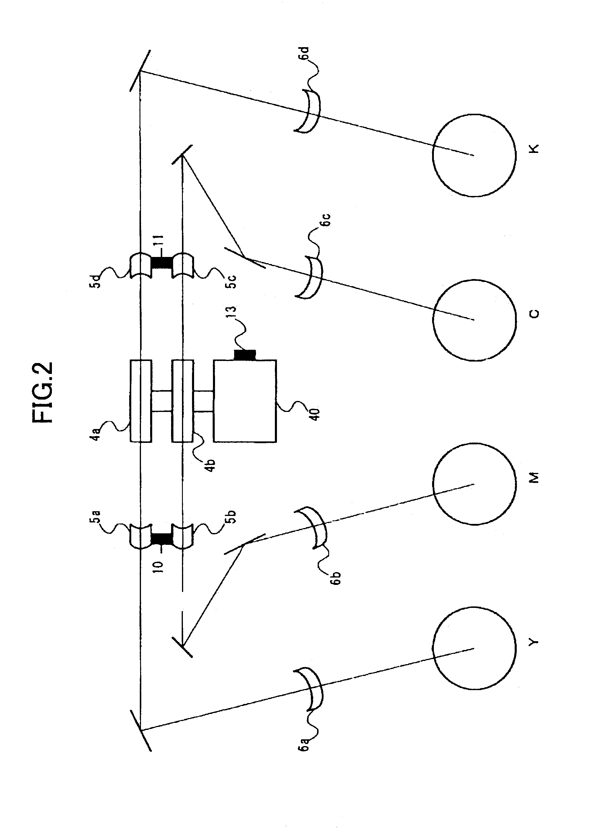
[0030]Hence, it is further object of the present invention to simplify correction control of print position shift by reducing the number of deflectors driven by rotating motors, the number of the deflectors being less than the number of media to be scanned so as to control self-generation of heat, and by detecting the temperature of a plurality of scan optical systems with a single temperature detecting element since the temperatures of physically close scan optical systems are almost equal.

Problems solved by technology

However, in the above-described conventional method of adjusting the registration, errors in reading the pattern for detecting the variation in registration are considerable.
Thus, there is a problem in that the registration correction cannot be correctly performed, and thus it is impossible to obtain a high quality image.
Additionally, since a CCD or the like for reading is required, there is also a problem in that the size of each of the laser scan optical units is increased and cost increases.
Further, in the method of standardizing the temperature characteristic of each of the laser scan optical units so as to perform the color matching of each of the laser scan optical units of the laser scan optical device, it is difficult to standardize the temperature characteristics due to limitations of accuracy of components.
This causes color shift.
However, in such a correction method, though it is possible to correct the shift in the sub scan direction introduced by the temperature change, there is a problem in that it is impossible to perform correction of shift of registration in the main scan direction.
However, in the prior art 3, the cost is high since the tandem laser scan optical device includes four sets of a light source, a polygon motor, a fθ lens, and a temperature sensor for four colors, that is, Y, M, C and K.
Accordingly, energy saving is not achieved.
Further, correction control is complex since the tandem laser scan optical device uses as many as four temperature sensors.
Especially, in color images, the variation in the scan speed causes color shift, resulting in degradation in color reproduction characteristics and resolution.
However, in prior art, there is a limit to eliminating the variation in the scan speed.

Method used


Image

  • Image forming method, image forming apparatus, optical scan device, and image forming apparatus using the same
  • Image forming method, image forming apparatus, optical scan device, and image forming apparatus using the same
  • Image forming method, image forming apparatus, optical scan device, and image forming apparatus using the same

Examples


first embodiment

[0122]FIG. 6 shows the configuration of the pixel clock phase adjusters (3a through 3d in FIG. 1). In FIG. 6, a high frequency clock generation circuit 1 generates a high frequency clock VCLK that is the basis of the pixel clock PCLK. A counter 1 (2) is a counter that operates when the clock VCLK rises. A comparator 1 (3) outputs a control signal 1 based on a result of comparison among a value of the counter 1 (2), a predetermined value, and a comparison value 1 output by a comparison value generation circuit 9. A clock 1 generation circuit 4 generates a clock 1 based on the control signal 1. A counter 2 (5) is a counter that operates when the clock VCLK falls. A comparator 2 (6) outputs a control signal 2 based on a result of comparison among a value of the counter 2 (5), a predetermined value, and a comparison value 2 output by the comparison value generation circuit 9. A clock 2 generation circuit 7 generates a clock 2 based on the control signal 2. A multiplexer (MUX) 8 selects ...

second embodiment

[0143]A description will be given of the second embodiment.

[0144]FIG. 11 shows the configuration of the pixel clock generation circuit according to the second embodiment. In the second embodiment, a phase data storing circuit 12 for storing a plurality of phase data is added to the configuration according to the first embodiment. Data of the phase data storing circuit 12 are set externally. The phase data storing circuit 12 sequentially outputs phase data in synchronization with the pixel clock PCLK.

[0145]In this manner, for example, in a case of data having the same phase data for each line, such as phase data for correcting unevenness in scanning caused by the characteristics of scan lens, by storing the phase data in the phase data storing circuit 12 beforehand, and sequentially outputting the phase data from the phase data storing circuit 12 every time a line is scanned, it is not necessary to input the same data to the phase data storing circuit 12 from the outside. Accordingly...

third embodiment

[0146]A description will be given of the third embodiment.

[0147]FIG. 12 shows the configuration according to the third embodiment. In the third embodiment, a phase data combining circuit 13 is added to the configuration according to the second embodiment. The phase data combining circuit 13 combines and outputs, to the comparison value generation circuit 9, external phase data given from the outside and internal phase data output from the phase data storing circuit 12. The phase data combining circuit 13 performs the calculation as shown below and outputs the phase data.

[0148]phase⁢⁢data=external⁢⁢phase⁢⁢data+internal⁢⁢phase⁢⁢data

[0149]Hence, it is possible not only to perform the same correction for every line, such as correcting unevenness in scanning caused by the characteristics of scan lens, but to perform a correction that varies in every line, such as correcting unevenness of the rotation of the polygon mirror.

[0150]Next, a description will be given of a light beam source use...


PUM


Abstract

An optical scan device having an optical deflector reflecting a light beam from a light beam source so as to deflect the light beam and having a surface to be scanned on which information is written such that the light beam deflected by the deflector scans the surface is disclosed. Optical detectors are arranged at least in two locations, a start side of writing and an end side of writing, which locations are outside an effective writing area. A measuring part measures a scan time required by the light beam deflected by the optical deflector to scan a range between the optical detectors. A correcting part corrects each dot position of image data in the effective writing area to an arbitrary position based on a variation amount of the measured scan time.

Description

BACKGROUND OF THE INVENTION[0001]1. Field of the Invention[0002]The present invention generally relates to image forming apparatuses such as laser printers, laser facsimiles, and digital copying machines, optical scan devices used for such image forming apparatuses, and image forming methods, and more particularly, to an image forming apparatus and image forming method that perform correction of a shift (displacement) of a scan position of laser scan, and pixel position control of optical scan devices.[0003]2. Description of the Related Art[0004]A color laser printer is equipped with a laser scan optical device having laser scan optical units corresponding to four colors (Y: yellow, M: magenta, C: cyan, and BK: black). Each of the laser scan optical units includes a laser diode emitting a laser light beam, a polygon mirror deflecting the laser beam, and the like.[0005]The laser beam emitted from-the laser diode is deflected by the polygon mirror after modulation based on image data,...

Claims


Application Information

Patent Timeline
Patent Type & Authority Patents(United States)
IPC IPC(8): B41J2/435B41J2/47G02B26/12
CPCB41J2/473G02B26/123
Inventor SUZUKI, SEIZOISHIDA, MASAAKIOMORI, ATSUFUMIAOKI, MAGANENIHEI, YASUHIRO
Owner RICOH KK
Learn More