Ultra-wideband antenna and ultrahigh frequency circuit module

a wideband antenna and ultrahigh frequency circuit technology, applied in waveguide devices, resonant antennas, protective material radiating elements, etc., can solve the problems of inability to achieve input impedance matching of antennas and hammering wideband characteristics, and achieve the effect of high frequency circuits and low reflection loss

Active Publication Date: 2007-09-04
CALLAHAN CELLULAR L L C
View PDF10 Cites 10 Cited by
  • Summary
  • Abstract
  • Description
  • Claims
  • Application Information

AI Technical Summary

Benefits of technology

[0017]More specifically, line widths are selected so that at sections where lecher wires and microstrip connection lines connect, the lecher wire impedance and the odd mode impedance cause reflection to be as small as possible at a desired bandwidth. As an example of this method, there is matching design theory using a lambda / 4 transformer. If this is done, at joints of the lines, it is possible to connect with no almost no reflection loss in the desired band.
[0022]According to the present invention, it is possible to realize an antenna with little reflection loss over an extremely wideband range, and a high frequency circuit (module) including the antenna.

Problems solved by technology

The major factor hampering wideband characteristics is widely known to be that input impedance matching of the antenna cannot be achieved.

Method used


Image

  • Ultra-wideband antenna and ultrahigh frequency circuit module
  • Ultra-wideband antenna and ultrahigh frequency circuit module
  • Ultra-wideband antenna and ultrahigh frequency circuit module

Examples


embodiment 1

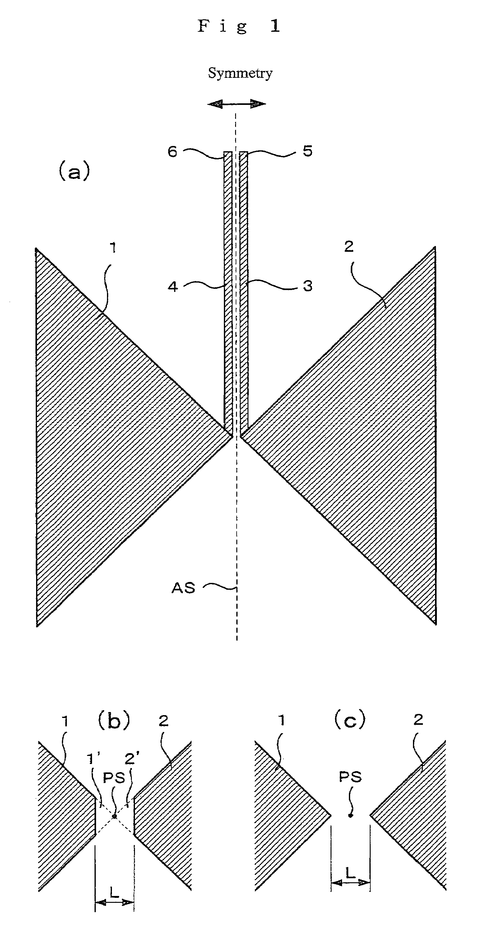
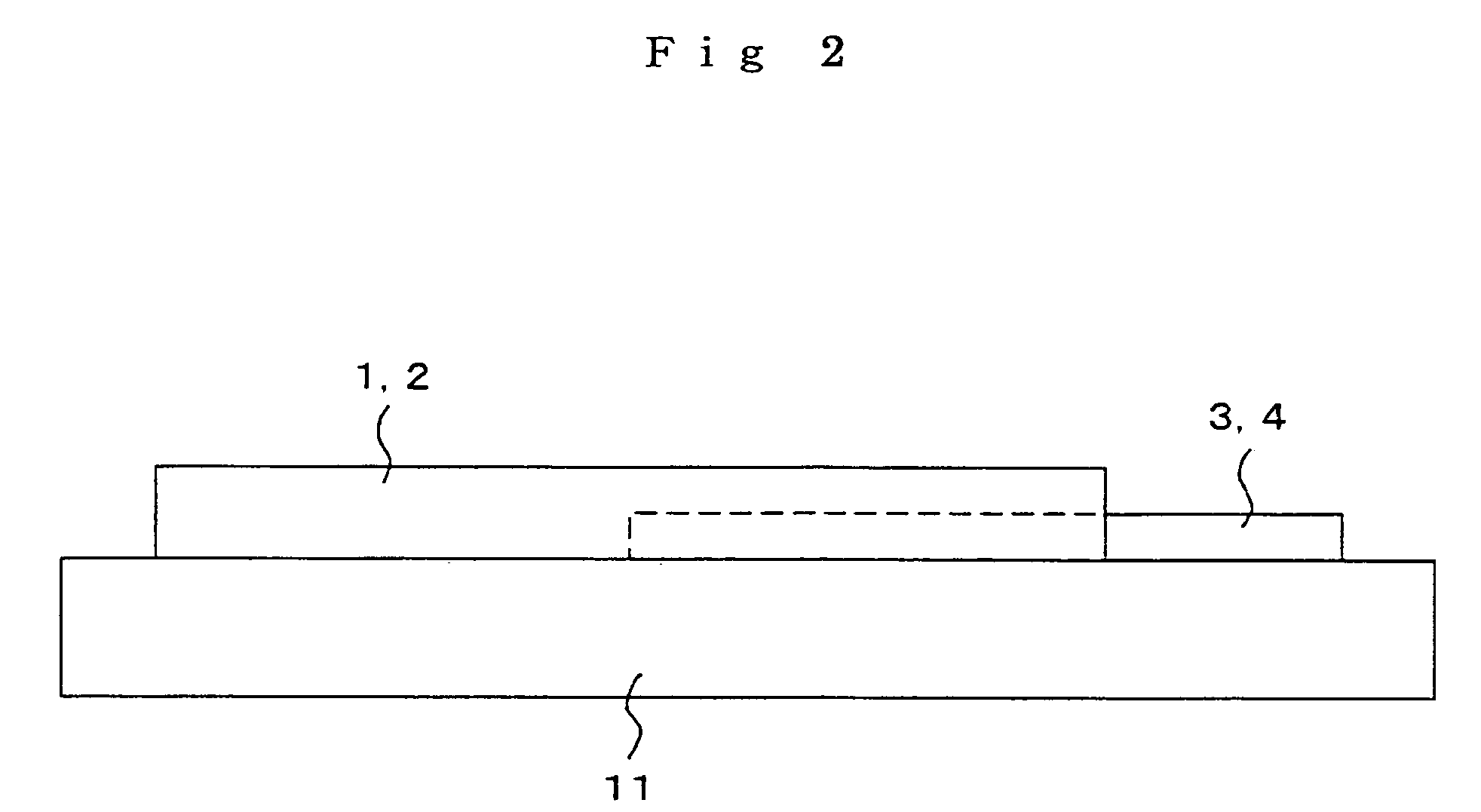
[0042]An antenna relating to embodiment 1 of the invention will now be described with reference to the drawings. FIG. 1(a) is a plan view of an antenna module relating to embodiment 1 of the invention. Reference numerals 1, 2 are antenna conductors constituting the antenna, and 3, 4 are feed conductors connected to respective one ends of the antenna conductors 1, 2. 5, 6 are ends of the feed conductors 3, 4 at an opposite side to the antenna conductors 1, 2. Signals that are 180 degrees out of phase with each other are fed from these sections 5, 6. The antenna conductors 1, 2 and the feed conductors 3, 4 are line symmetrical about an axis of symmetry AS.

[0043]FIG. 1(b) is an expanded drawing of a central part of the antenna. FIG. 1(c) shows another variation of the central part of the antenna. In FIG. 1(b) and FIG. 1(c), the feed conductors 3, 4 are omitted. A point of symmetry PS exists between the antenna conductors 1 and 2, with the antenna conductors 1 being 2 rotationally symme...

embodiment 2

[0061]With embodiment 1 of the present invention, a dielectric substrate is provided on one surface of the antenna conductor, but it is also possible to provide a dielectric substrate on both surfaces. Examples of embodiment 2 of the present invention are shown in FIG. 9 and FIG. 10. In these drawings, the same reference numerals are attached to sections that are the same as or correspond to those in the above-described embodiment.

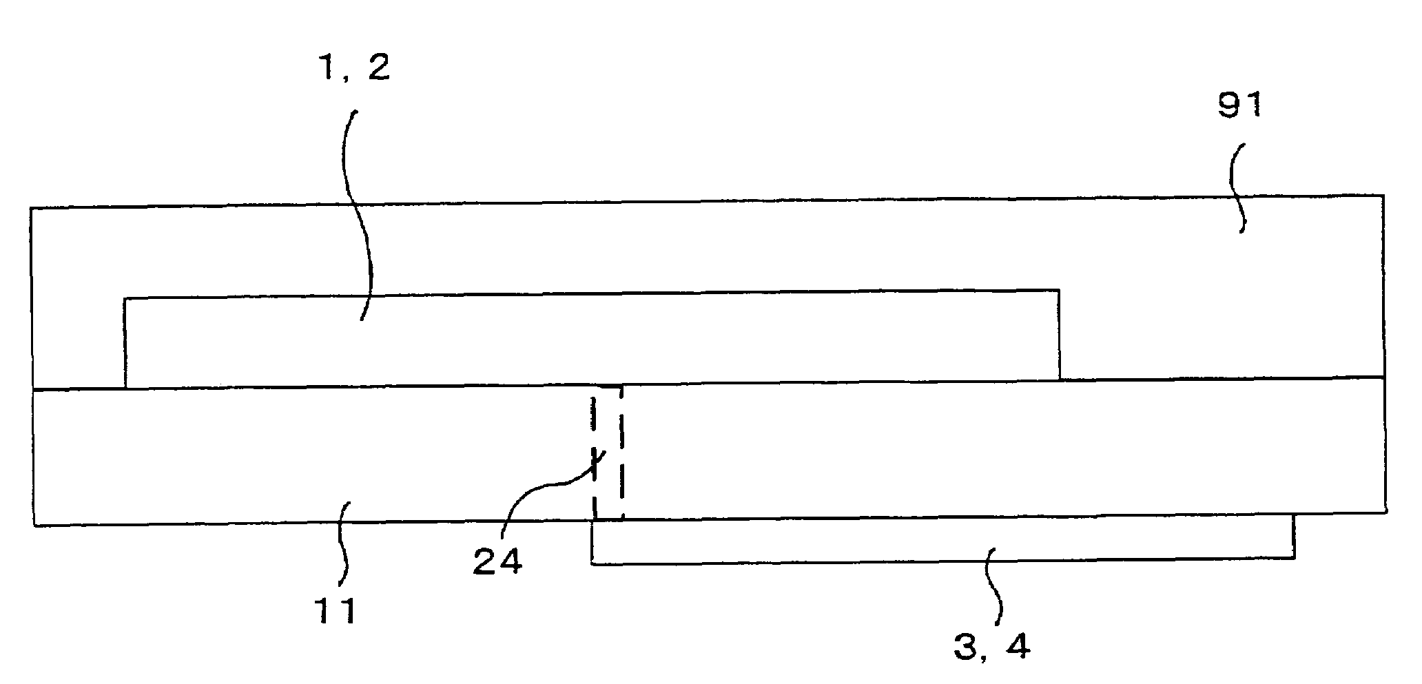
[0062]FIG. 9 is a plan view of an antenna module relating to embodiment 2 of the invention. The feed conductors 3, 4 are provided on a rear surface on the dielectric substrate. As a result, via-holes 24, 24 are provided in order to connect the antenna conductors 1, 2 and the feed conductors 3, 4. Signals that are 180 degrees out of phase with each other are fed from sections 5, 6.

[0063]FIG. 10 is a right side view of an antenna module relating to embodiment 2 of the invention. Reference numeral 91 is a second dielectric substrate provided on the antenna co...

embodiment 3

[0068]It is possible to endow the feed conductors with a impedance conversion function. Examples of embodiment 3 of the present invention are shown in FIG. 12. FIG. 12 is a plan view of an antenna module relating to embodiment 3 of the invention. In this drawing, the same reference numerals are attached to sections that are the same as or correspond to those in the above-described embodiment.

[0069]In FIG. 12, reference numerals 37 and 38 are antenna conductor 1, 2 side ends of the feed conductors 3, 4, and the feed conductors 3, 4, are electrically connected to the antenna conductors 1, 2 at these sections. The antenna conductors 1, 2 and the feed conductors 3, 4 are symmetrical about a plane of symmetry, signals that are 180 degrees out of phase are fed from ends 5, 6 of the feed conductors opposite to the antenna, and this point is the same as for the case of embodiment 1 of the invention.

[0070]In embodiment 3 of the invention, if the width of the end 5 of the feed conductor 3 is ...


PUM


Abstract

One of the objects of this invention is to realize an antenna having low reflection loss over an extremely wideband. The antenna of the present invention is provided with a dielectric substrate, a plurality of antenna conductors formed on one surface of the dielectric substrate that are pseudo self-complementary on the surface, and a plurality of feed conductors symmetrical with respect to symmetrical surfaces of the antenna conductors, wherein a gap for a wavelength of 1 / 10 or less that of the wavelength of a usage frequency in a vacuum is provided at a center of rotational symmetry between the plurality of antenna conductors.

Description

BACKGROUND OF THE INVENTION[0001]1. Field of the Invention[0002]This invention relates to an ultra wideband antenna and an ultrahigh frequency circuit module that can be applied to an ultra-wideband wireless system or the like to enable high speed transmission.[0003]2. Description of the Related Art[0004]In recent years, close range wireless interfaces such as wireless LANs and Bluetooth (trademark) have become widely used, but ultra-wideband wireless systems (UWB) have been receiving attention as the next generation of systems to enable even higher speed transmission. Specification investigations are currently progressing in various countries, but it is recognized that the usage frequency for these UWB systems in the US is 3.1-10.6 GHz with a comparatively large output. This UWB system is capable of high speed wireless transmission at 100 Mbps or above due to use of high frequencies in an extremely wide band, but it is not easy to implement an antenna for transmission of this type ...

Claims


Application Information

Patent Timeline
Patent Type & Authority Patents(United States)
IPC IPC(8): H01Q1/38H01Q9/28H01P5/08H01Q1/40H01Q19/09
CPCH01Q1/38H01Q9/28H01Q19/09
Inventor SAITOU, AKIRAHONJO, KAZUHIKO
Owner CALLAHAN CELLULAR L L C
Why Eureka
Try Eureka