Ultra-wideband antenna and ultrahigh frequency circuit module
- Summary
- Abstract
- Description
- Claims
- Application Information
AI Technical Summary
Benefits of technology
Problems solved by technology
Method used
Image

Examples
embodiment 1
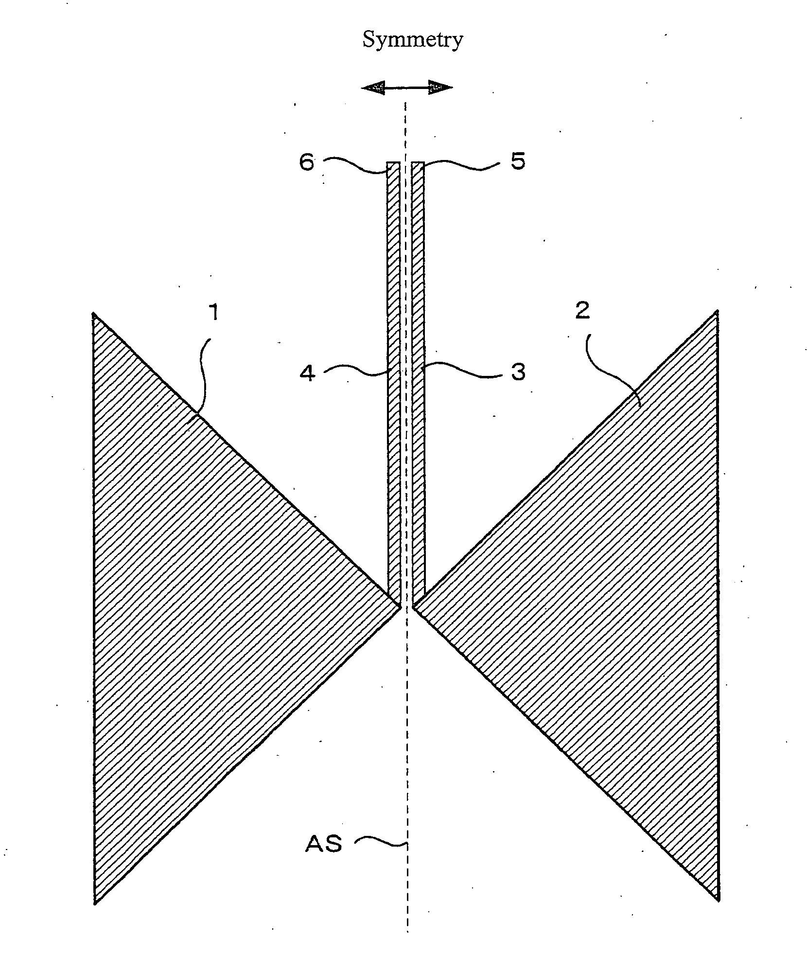
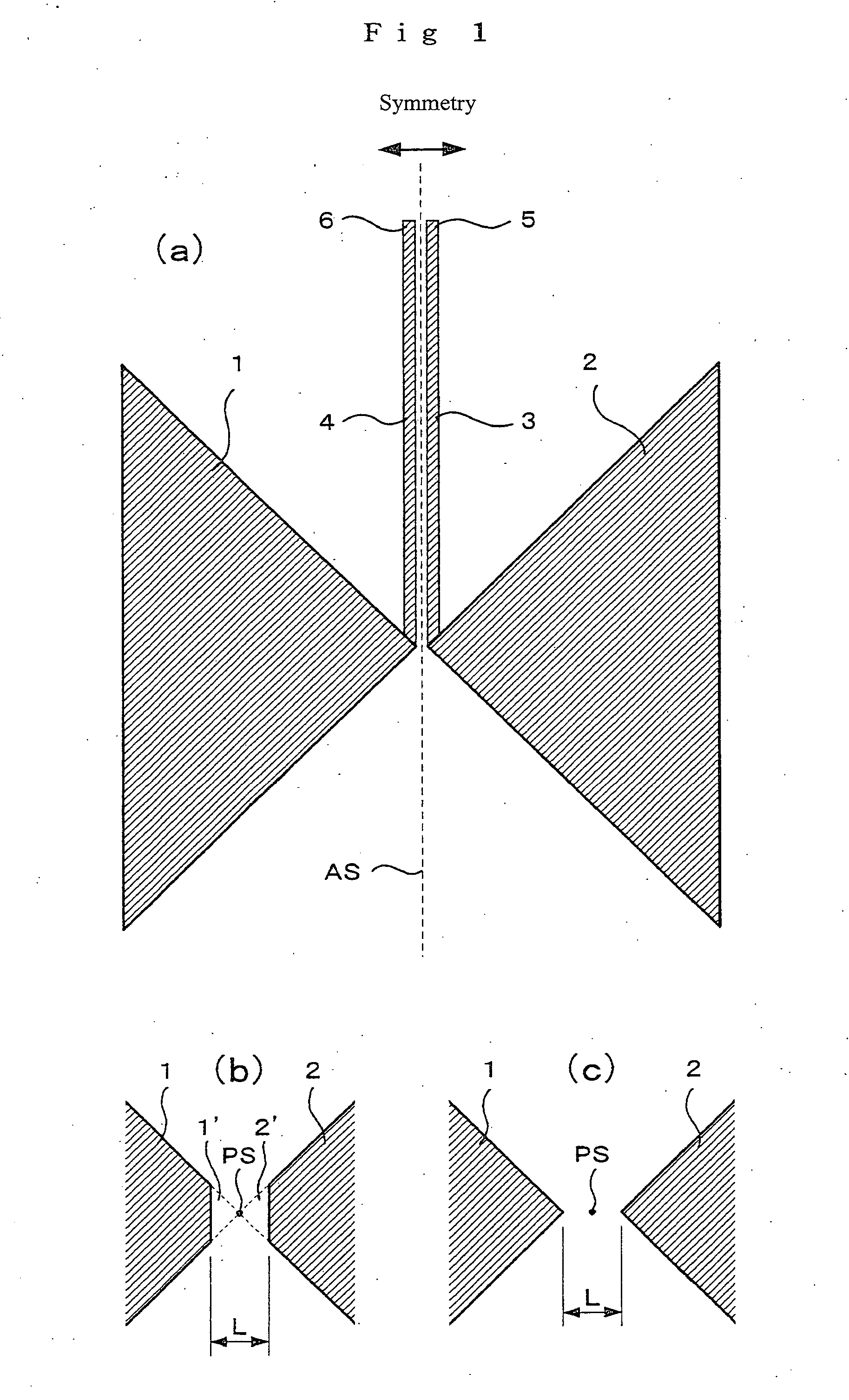
[0042] An antenna relating to embodiment 1 of the invention will now be described with reference to the drawings. FIG. 1(a) is a plan view of an antenna module relating to embodiment 1 of the invention. Reference numerals 1, 2 are antenna conductors constituting the antenna, and 3, 4 are feed conductors connected to respective one ends of the antenna conductors 1, 2, 5, 6 are ends of the feed conductors 3, 4 at an opposite side to the antenna conductors 1, 2. Signals that are 180 degrees out of phase with each other are fed from these sections 5, 6. The antenna conductors 1, 2 and the feed conductors 3, 4 are line symmetrical about an axis of symmetry AS.
[0043]FIG. 1(b) is an expanded drawing of a central part of the antenna. FIG. 1(c) shows another variation of the central part of the antenna. In FIG. 1(b) and FIG. 1(c), the feed conductors 3, 4 are omitted. A point of symmetry PS exists between the antenna conductors 1 and 2, with the antenna conductors 1 being 2 rotationally sym...
embodiment 2
[0061] With embodiment 1 of the present invention, a dielectric substrate is provided on one surface of the antenna conductor, but it is also possible to provide a dielectric substrate on both surfaces. Examples of embodiment 2 of the present invention are shown in FIG. 9 and FIG. 10. In these drawings, the same reference numerals are attached to sections that are the same as or correspond to those in the above-described embodiment.
[0062]FIG. 9 is a plan view of an antenna module relating to embodiment 2 of the invention. The feed conductors 3, 4 are provided on a rear surface on the dielectric substrate. As a result, via-holes 24, 24 are provided in order to connect the antenna conductors 1, 2 and the feed conductors 3, 4. Signals that are 180 degrees out of phase with each other are fed from sections 5, 6.
[0063]FIG. 10 is a right side view of an antenna module relating to embodiment 2 of the invention. Reference numeral 91 is a second dielectric substrate provided on the antenna...
embodiment 3
[0068] It is possible to endow the feed conductors with a impedance conversion function. Examples of embodiment 3 of the present invention are shown in FIG. 12. FIG. 12 is a plan view of an antenna module relating to embodiment 3 of the invention. In this drawing, the same reference numerals are attached to sections that are the same as or correspond to those in the above-described embodiment.
[0069] In FIG. 12, reference numerals 37 and 38 are antenna conductor 1, 2 side ends of the feed conductors 3, 4, and the feed conductors 3, 4, are electrically connected to the antenna conductors 1, 2 at these sections. The antenna conductors 1, 2 and the feed conductors 3, 4 are symmetrical about a plane of symmetry, signals that are 180 degrees out of phase are fed from ends 5, 6 of the feed conductors opposite to the antenna, and this point is the same as for the case of embodiment 1 of the invention.
[0070] In embodiment 3 of the invention, if the width of the end 5 of the feed conductor ...
PUM
 Abstract
Description
Claims
Application Information