Layered product, luminescence device and use thereof

a luminescence device and product technology, applied in the manufacture of discharge tubes/lamps, electrode systems, discharge tubes, etc., can solve the problems of low adhesion, defect, and easy peeling of both films, and achieve good water vapor barrier properties, good scratch resistance, and good light transmission

Active Publication Date: 2013-10-01
ZEON CORP
View PDF8 Cites 6 Cited by
  • Summary
  • Abstract
  • Description
  • Claims
  • Application Information

AI Technical Summary

Benefits of technology

[0060]The layered product in the invention has a good water vapor barrier property, and good scratch resistance, which can be favorably employed for not only a wrapping material but also a sealing layer of electronics devices such as a luminescence device represented by an organic EL device.
[0061]Also the layered product in the invention is little in reflection loss, high in efficiency of light production, long in life of light emission, good in water vapor barrier property and good in scratch resistance of the surface, which can be favorably employed for a back light unit or a plane light-source of a segment display, dot matrix display, and liquid crystal display.

Problems solved by technology

But, as the result of our review, the film has low adhesion between resin film and inorganic film, so we found that both films are easily peeled off.
This peel-off may easily bring about a defect such as crack in the inorganic film, being to lower gas barrier property.
Not less than eight layers of the inorganic film and the resin film are required to be enough gas barrier property, so it is dissatisfied with productivity thereof.
As the result of our review, however, use of only means for resolution described in patent document 3 is to result in insufficiency of adhesion between resin film and inorganic film yet.
However, in an organic EL device, using of material for negative electrode being low in work function easily causes the negative electrode to be corroded or oxidized by reacting with water-vapor or oxygen in air.
This degradation of the negative electrode results in sprouting non-emission region called as “dark spot” in the luminescent-material layer, causing organic EL device to degrade in the property by aging.
But, the film made of the above material needs large thickness for improvement of water-vapor resistance, which causes elevating internal strain easily to make crack in film, being likely to reduce the sealing performance by contraries.
But, adhesion between organic matter and silicon oxynitride is extremely low without limitation of chemical structure or film making method, so the peel-off brings about defect in an interface to lower sealing property.
But, applying of the decomposition polymer alone on the organic EL device results in having yet been insufficient sealing property, so it needs more improvement.[Patent Document 1] JP-A-2003-206361[Patent Document 2] JP-A-2003-48271[Patent Document 3] JP-A-2002-234103[Patent Document 4] JP-A-H10-261487[Patent Document 5] JP-A-2002-25765[Patent Document 6] JP-A-2002-56971

Method used


Image

  • Layered product, luminescence device and use thereof
  • Layered product, luminescence device and use thereof
  • Layered product, luminescence device and use thereof

Examples


example 1

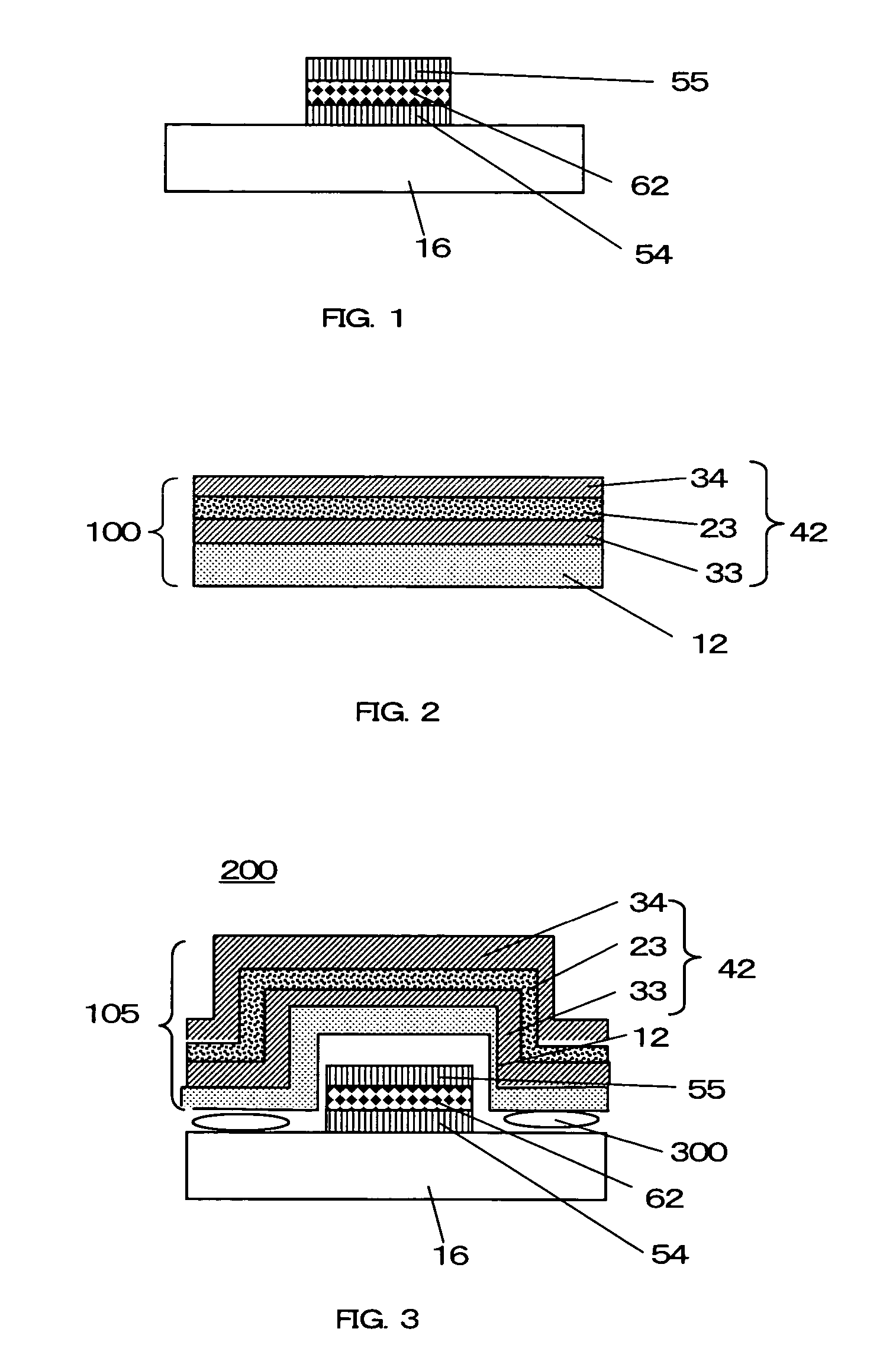
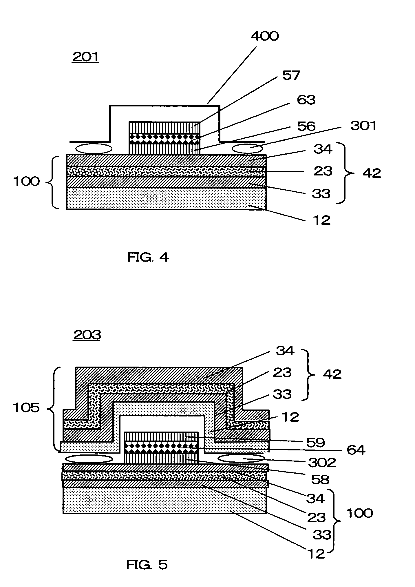
[0185]FIG. 2 is cross section of layered product in Example 1 to 2.

[0186]In Example 1, as transparent resin substrate 12 was used film (ZEONOR FILM ZF-14, thickness=100 μm, produced by Zeon Corp.) made from norbornene based polymer being one of alicyclic structure containing polymers. SiO2 as target material was deposited on the substrate by RF sputtering process to make an inorganic film 33 having average thickness of 200 nm. Then norbornene based polymer (ZEONOR 1600 produced by Zeon Corp., “COP” in table) being one of alicyclic structure containing polymers was provided at film making rate of 90 nm / min, and SiO2 was simultaneously provided at film making rate of 10 nm / min, by electron beam vapor deposition process to make an organic film 23 having thickness of 1 μm on the above inorganic film. And SiO2 as target material was deposited on the above organic film by RF sputtering process to make an inorganic film34 having average thickness of 200 nm, which results obtaining a layere...

example 2

[0188]In EXAMPLE 2, as transparent resin substrate 12 was used film (ZEONOR FILM ZF-14, thickness=100 μm, produced by Zeon Corp.) made from norbornene based polymer being one of alicyclic structure containing polymers. The substrate was winded on a winding-off roll 501 in continuous vacuum sputtering system (direct current magnetron sputtering system) as shown in FIG. 10. Silicon dioxide was filled in target 506 and 509.

[0189]Then, vacuum exhausting from vacuum chamber 500 was begun to reach to 1×10⁻⁵ Pa in pressure. The transparent resin substrate was winded off from winding-off roll 501 at 0.1 m / min in velocity, silicon dioxide film having thickness of 200 nm was formed by sputtering from target 506 on condition that the traveled film on the deposition roll 503 was loaded with tension of 30 N. Tetrafluoromethane (CF4) and tetraethoxysilane (TEOS) were flowed from inlet line 7, at respectively 0.101 Pa·m3 / sec and 0.0676 Pa·m3 / sec (flow ratio by volume 60:40) under plasma by applyin...

example 3

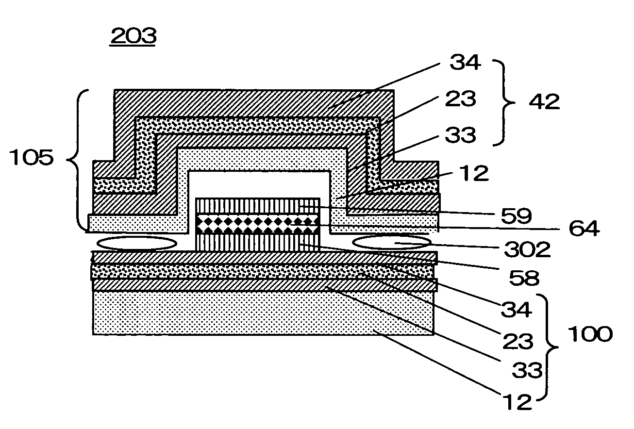
[0197]FIG. 3 is cross section of luminescence device in Examples 3 to 4.

[0198]In a resistance heater with reduced pressure of 10−4 Pa or less, Al as lower electrode layer 54 having thickness of 100 nm, lithium fluoride as electron injection layer (no illustration in the figures) having thickness of 1 nm, hydroxyquinoline aluminum (thereafter, Alq3) as luminescent-material layer 62 having thickness of 60 nm, and allylamine derivative (α-NPD) as positive transport layer (no illustration in the figures) having thickness of 40 nm were deposited in turn on a glass substrate 16. This deposition rate was 0.5 nm / min. In a DC sputtering device with reduced pressure of 10−4 Pa or less, ITO as upper electrode layer 55 having thickness of 200 nm was deposited. This deposition rate was 30 nm / min.

[0199]Then, the layered product 100-1 obtained in EXAMPLE 1, in state that the transparent resin substrate was faced, was pasted with an epoxy cement 300, so as to cover from the lower electrode layer 54...


PUM

PropertyMeasurementUnit
volume ratioaaaaaaaaaa
wave lengthaaaaaaaaaa
particle diameteraaaaaaaaaa

Abstract

A layered product comprising: sealing film comprising a laminate of at least one organic film and at least one inorganic film, and transparent resin substrate; in which the organic film is made from fluorine compound or alicyclic structure containing polymer and metallic simple substance or metallic compound as raw material, and in which the inorganic film is made from metallic simple substance or metallic compound as raw material. A luminescence device comprising: substrate, and lower electrode layer, luminescent-material layer, upper electrode layer and sealing film which are laminated in turn on the substrate; in which the substrate and the sealing layer comprises the layered product.

Description

TECHNICAL FIELD[0001]The invention relates to a layered product which can intercept oxygen, water vapor or so on, a luminescence device such as organic electroluminescence device (thereafter, “organic EL device”), and use thereof.BACKGROUND ART[0002]Gas barrier film is noticed as not only wrapping material for foods or medicine but also substrate of electronics devices, as the film is good in thinness, lightness and flexibility. Particularly, the film is noticed as the substrate for liquid crystal display or organic EL display which is looked for application to wall-hanging television or electronic paper. The gas barrier film is usually obtained by laminating gas-barrier layer on a transparent resin film substrate.[0003]There are various suggestions concerning the gas-barrier layer. For instance, in patent document 1 or patent document 2 is described gas barrier film comprising an alternate laminate of inorganic films comprising inorganic oxide such as SiO2 and Al2O3, and films comp...

Claims


Application Information

Patent Timeline
Patent Type & Authority Patents(United States)
IPC IPC(8): H01J9/26B32B9/00B32B19/00H01J63/04H01J1/62H01J9/32B32B27/00C23C28/00H05B33/04H05B33/14
CPCB32B27/00B32B15/08H05B33/04
Inventor YAMADA, YASUMIKASHIWAGI, MOTOFUMI
Owner ZEON CORP
Why Eureka
Try Eureka