Composite substrate material and process for producing the same

a substrate material and composite technology, applied in the field of composite substrate materials, can solve the problems of optical scattering and reflection loss, low long-term reliability of adhered areas, and high cost, and achieve high bond strength and long-term reliability of bonded areas. , good environmental temperature resistance characteristics

Inactive Publication Date: 2005-11-17
FUJIFILM CORP
View PDF12 Cites 0 Cited by
  • Summary
  • Abstract
  • Description
  • Claims
  • Application Information

AI Technical Summary

Benefits of technology

[0009] The primary object of the present invention is to provide a process for producing a composite substrate material, wherein wet processing need not be performed, and a composite substrate material having a high bond strength, high long-term reliability of a bonded area, and good environmental temperature resistance characteristics is capable of being produced.
[0010] Another object of the present invention is to provide a composite substrate material having a high bond strength, high long-term reliability of a bonded area, and good environmental temperature resistance characteristics of the bonded area.
[0019] With the process for producing a composite substrate material in accordance with the present invention, when each of the functional films having the photo-catalytic effects, such as metal oxide films, typically TiO2, is exposed to the light having a wavelength falling within the absorption wavelength range of the functional film, the photo-catalytic effects of the functional film occur. As a result, organic substances, and the like, which cling to the surface of each of the substrate materials, are decomposed approximately perfectly, and a super-hydrophilic state occurs on the surface of each of the substrate materials. Thereafter, the substrate materials are combined with each other such that the surfaces of the substrate materials, which surfaces are provided with the functional films, stand facing each other. Also, a load and heat are applied to the combined substrate materials. In this manner, the substrate materials are bonded to each other with a high bond strength. The bonded area has high long-term reliability and good environmental temperature resistance characteristics.
[0020] Further, with the process for producing a composite substrate material in accordance with the present invention, wherein wet processing need not be performed, the effects described above can be obtained easily.
[0021] Particularly, with the process for producing a composite substrate material in accordance with the present invention, wherein each of the functional films also acts as the anti-reflection film, a composite substrate material, which is substantially free from reflection loss at the bonded area or exhibits little reflection loss at the bonded area, can be obtained. Also, with the process for producing a composite substrate material in accordance with the present invention, wherein each of the functional films is formed thin such that each of the functional films is optically negligible, a composite substrate material, which is substantially free from scattering loss at the bonded area or exhibits little scattering loss at the bonded area, can be obtained.
[0022] In this manner, for example, a reflectivity at the bonded area of a plurality of optical substrates (or crystals) can be limited easily and reliably to a value of approximately at most 0.2%. Also, it becomes possible to directly bond laser crystals, optical wavelength converting crystals, or other crystals in solid lasers, and the like, to each other. Therefore, with the process for producing a composite substrate material in accordance with the present invention, a subminiature solid laser having reliable performance can be furnished.

Problems solved by technology

However, the techniques, wherein the optical crystals or the optical substrates are adhered to each other by optical adhesive agents, have the problems in that optical scattering and reflection loss are caused to occur and long-term reliability of the adhered areas is low.
Particularly, as for optical members to be located within laser resonators, the problems described above arise markedly.
The techniques, wherein the optical crystals or the optical substrates are fusion bonded under heat, have the problems in that the techniques are applicable only to limited combinations of materials and can be utilized only in limited applications.
However, the wafer bonding techniques have the problems in that wet processing must be performed for cleaning the substrates and therefore production steps cannot be kept simple.

Method used


Image

  • Composite substrate material and process for producing the same
  • Composite substrate material and process for producing the same

Examples


Embodiment Construction

[0024] The present invention will hereinbelow be described in further detail with reference to the accompanying drawings.

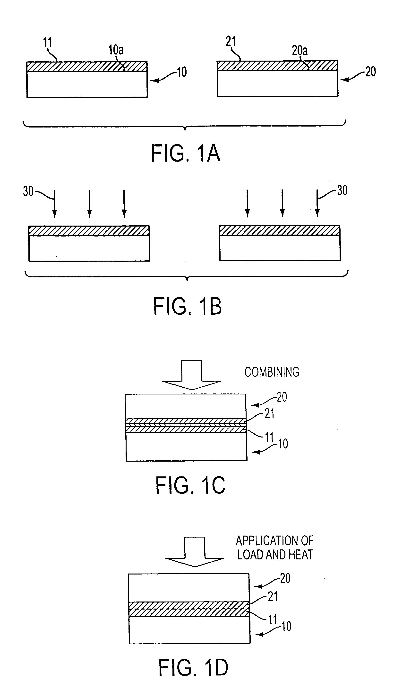
[0025]FIGS. 1A, 1B, 1C, and 1D show steps in a first embodiment of the process for producing a composite substrate material in accordance with the present invention.

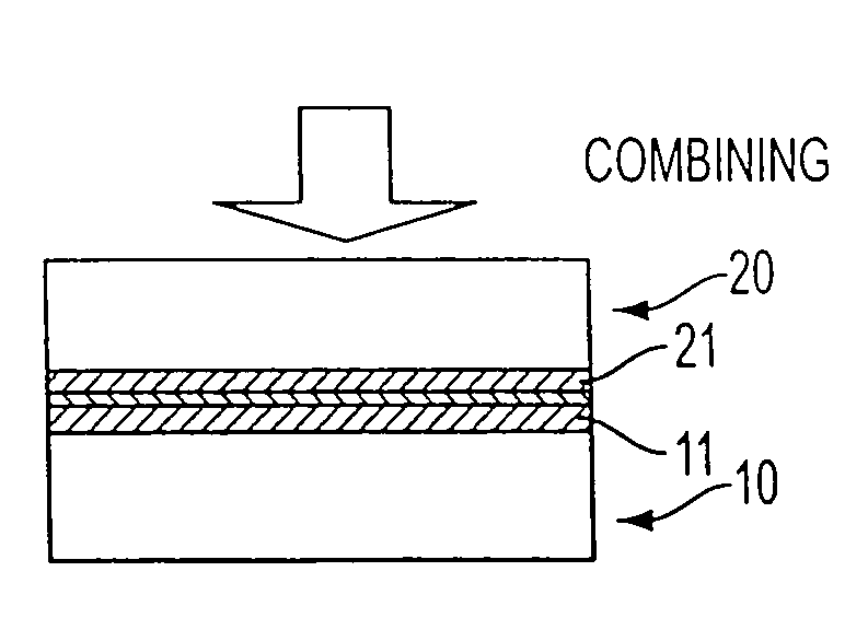
[0026] Firstly, as illustrated in FIG. 1A, two Si wafers 10 and 20, which act as substrate materials, are prepared. The Si wafers 10 and 20 respectively have surfaces 10a and 20a, which have been subjected to mirror finish. Thereafter, TiO2 thin films 11 and 21, which act as functional films having photo-catalytic effects, are respectively formed on the surfaces 10a and 20a. In this embodiment, each of the Si wafers 10 and 20 has a thickness of 300 μm. Also, the TiO2 thin films 11 and 21 can be formed with, for example, a sputtering technique or a sol-gel technique.

[0027] Thereafter, as illustrated in FIG. 1B, the surface of each of the TiO2 thin films 11 and 21 is exposed to ultraviolet light 30 ha...


PUM

PropertyMeasurementUnit
reflectivityaaaaaaaaaa
thicknessaaaaaaaaaa
wavelengthaaaaaaaaaa

Abstract

A functional film, which has photo-catalytic effects, is overlaid on a surface of each of at least two substrate materials. The functional film, which has been overlaid on the surface of each of the substrate materials, is exposed to light having a wavelength falling within an absorption wavelength range of the functional film. The substrate materials are then bonded to each other with the functional films, which have been exposed to the light, intervening between the substrate materials. The functional film may be a film containing TiO2, and the light irradiated to the functional film may be ultraviolet light. In cases where a film other than the functional film is also overlaid on the surface of each of the substrate materials, the functional film is formed as a top layer.

Description

BACKGROUND OF THE INVENTION [0001] 1. Field of the Invention [0002] This invention relates to a composite substrate material comprising at least two substrates which are bonded to each other. This invention also relates to a process for producing the composite substrate material. [0003] 2. Description of the Related Art [0004] Composite materials have heretofore been formed by bonding optical crystals, such as laser crystals, optical wavelength converting crystals, and quartz glass mirrors, to each other or by bonding optical substrates to each other. As techniques for the bonding, techniques, wherein the optical crystals or the optical substrates are adhered to each other by optical adhesive agents, or techniques, wherein the optical crystals or the optical substrates are fusion bonded under heat, have heretofore been used widely. [0005] However, the techniques, wherein the optical crystals or the optical substrates are adhered to each other by optical adhesive agents, have the pro...

Claims


Application Information

Patent Timeline
Patent Type & Authority Applications(United States)
IPC IPC(8): C04B37/02B01J35/00B01J37/02B32B9/00B32B9/04B32B17/06B32B27/00C03C27/00C03C27/06C04B37/04G02B7/00
CPCB01J21/063B01J35/004B01J37/0215B01J37/0244B32B17/06Y10T428/252C03C27/00C03C27/06C03C2217/71G02B7/00B32B27/00Y10T428/31504Y10T428/8305
Inventor HARADA, AKINORI
Owner FUJIFILM CORP
Why Eureka
Try Eureka