Generation of test vectors for testing electronic circuits taking into account of defect probability

a technology of defect probability and test vector, which is applied in the field of generation, can solve the problems of high percentage fault coverage, affecting the manufacturing and testing of ic chips, and the probability of any node being shorted or mis-wired to any other node is unpredictable or at least very difficult to characterize, so as to reduce the number of test vectors required. the effect of reducing the number of vectors

Inactive Publication Date: 2007-09-04
LUK FONG
View PDF5 Cites 11 Cited by
  • Summary
  • Abstract
  • Description
  • Claims
  • Application Information

AI Technical Summary

Benefits of technology

[0011]Specifically, it is an object of the present invention to provide a new IC testing technique for generating testing pattern signals weighted by the fault probability to greatly simplify and reduce the number of testing vectors required for conducting the IC functionality tests.

Problems solved by technology

As the integrated circuits (ICs) and other form of electronic circuits become more complicate with higher level of integration and increasingly faster operational speed, the traditional techniques of the circuit testing configurations and methods are challenged by many technical difficulties.
One of the major difficulties is the concept of “fault-coverage” in an attempt to more thoroughly and completely test the electronic circuits supported on either a semiconductor wafer or on other circuit support platforms applying various fabrication processes.
However, as the IC chips and electronic device becomes miniaturized to include large number of different transistors and accompanied circuits, high percentage fault coverage becomes an extreme heavy burden on the manufacturing and testing of the IC chips.
In this type of process, the probability of any node being shorted or mis-wired to any other node is unpredictable or at the least very hard to characterize.
However in that time, all the system complexity is very low in terms of test equipment capability.
Due to the rapid development of very large-scale integrated circuit (VLSI) and system on chip (S.O.C) technology, the extreme circuit complexity of state of art VLSI and S.O.C. has made testability becoming a major issue in the production process.
The conventional pattern generation algorithm guided by fault coverage theory has come to a point that an astronomical number of test patterns are required to produce sufficient test coverage and that leads to the use of complex device to carry out very costly tests.
In increasing numbers of cases, the test requirement becomes too complicate and not practical or economically not viable even by using those most advance test equipments.
However, even with the benefits of reduced volume of testing data, as more testing points are added for the purpose of reducing the volume of test data, additional costs and time are required for carrying out the tests to include those inserted testing points.
To overcome this manufacturing bottle neck, a variety of testing techniques have been adapted such as BIST which needs additional circuitry to be incorporated into the device during early design stage thus costing not only silicon real state and design engineering time but also affecting device performance and capacity.
Some other techniques such as IDDQ can only provide limited improvement but are not effective enough to remedy the problem significantly.
All prior art have fault coverage as the goal and measurement of effectiveness, but in current production environment, different sets of test pattern with same fault coverage may have different numbers of malfunction device undetected in the same lot of devices.

Method used


Image

  • Generation of test vectors for testing electronic circuits taking into account of defect probability
  • Generation of test vectors for testing electronic circuits taking into account of defect probability
  • Generation of test vectors for testing electronic circuits taking into account of defect probability

Examples


Embodiment Construction

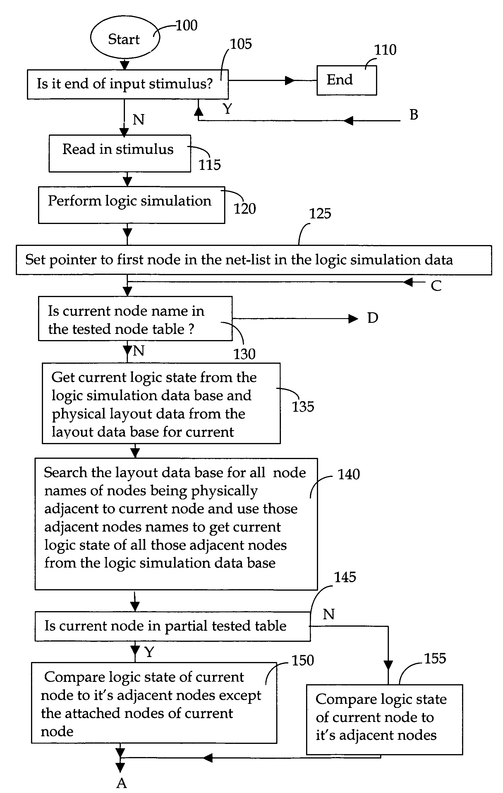
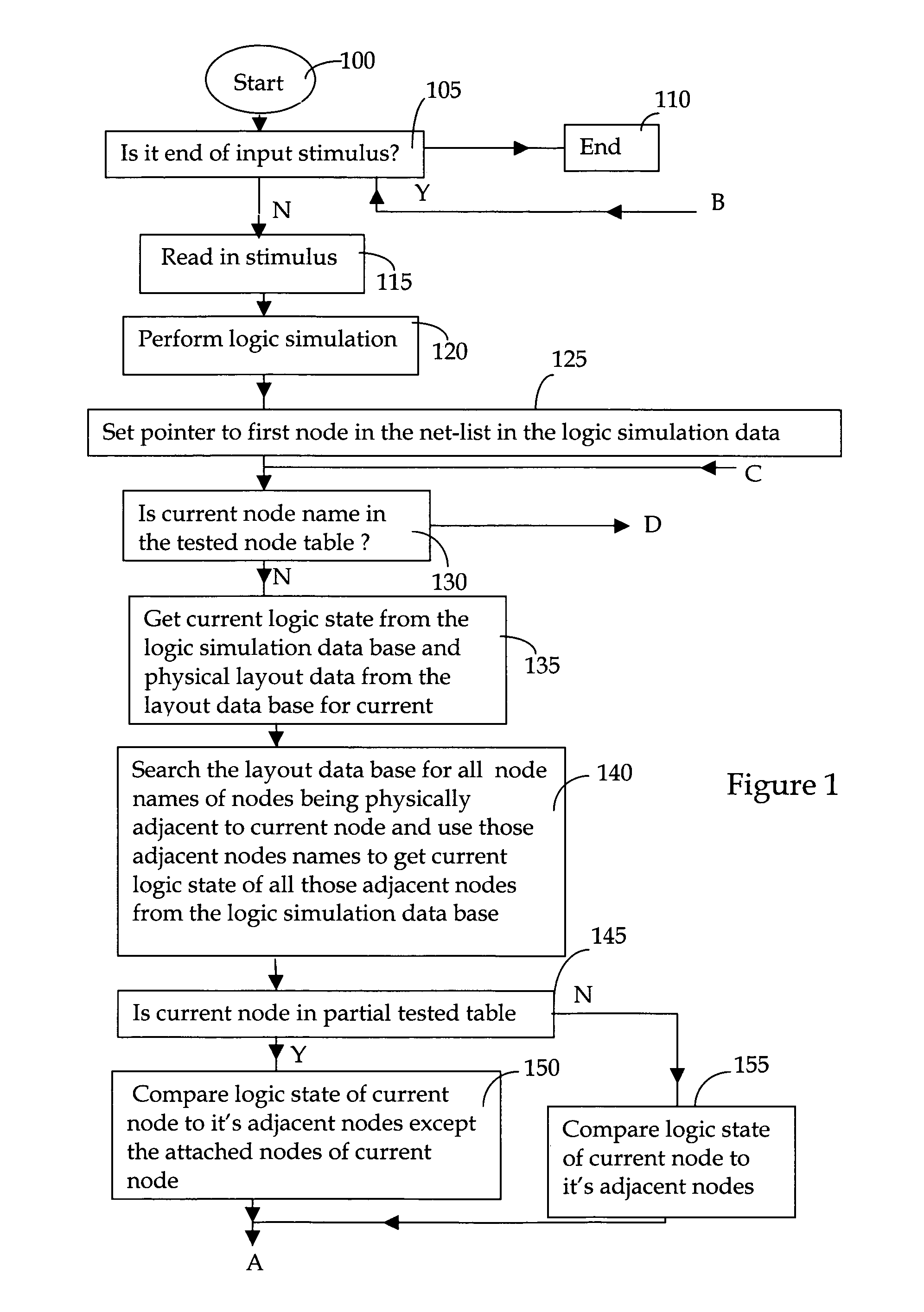
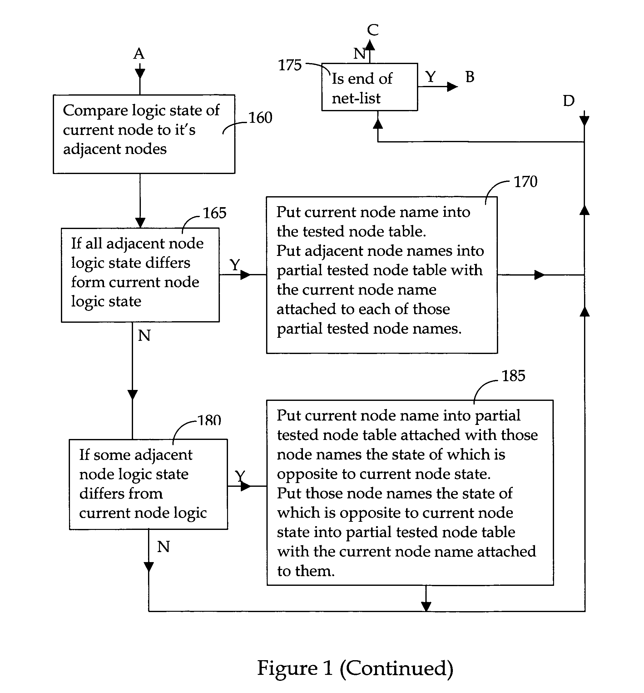
[0016]The present novel invention is different and totally non-obvious when compared to the conventional wisdom of fault coverage theory. Instead of focusing on detection of all faults or maximum number of faults, it takes into the account of the characteristics of modern day technologies of manufacturing processes for the printed circuit board and integrated circuit. A new approach is implemented to detect potential defects of circuits or circuit connectivity by taking into account the defect probability and defect density. Typically there are three types of failures that commonly cause circuit faults. The first two types, the internal circuit continuity, i.e., broken traces, within a node and excessive leakage between nodes are much less of a problem for testing. An internal circuit continuity test can be simply carried out by driving the respective nodes to two different states, i.e., 1 and 0's in binary logic system, and measuring output for correct responses. Simply driving the...


PUM


Abstract

A method for generating test pattern signals weighted by the fault probability to greatly simplify the test process and to reduce the number of test vectors required for conducting the integrated circuit functionality tests. The method takes into consideration that the electrical short conditions occur mostly between adjacent nodes. The “fault coverage” concept is revised to test faults occurred between adjacent nodes and the test vectors are generated based a fault-probability weighted algorithm such that tests are conducted mostly on connections between adjacent nodes either on a same horizontal layer of between vertical nodes having vertical overlapping areas.

Description

BACKGROUND OF THE INVENTION[0001]1. Field of the Invention[0002]This invention relates generally to the method and system of testing the electronic circuits including the integrated circuits (ICs). More particularly, this invention relates to an improved system configuration and method for simplifying and expediting the testing processes for electronic circuits including integrated circuits (ICs) by applying an improved algorithm by taking into account the defect probability as a key factor for generating the testing vector.[0003]2. Description of the Prior Art[0004]As the integrated circuits (ICs) and other form of electronic circuits become more complicate with higher level of integration and increasingly faster operational speed, the traditional techniques of the circuit testing configurations and methods are challenged by many technical difficulties. One of the major difficulties is the concept of “fault-coverage” in an attempt to more thoroughly and completely test the electron...

Claims


Application Information

Patent Timeline
Patent Type & Authority Patents(United States)
IPC IPC(8): G01R31/28
CPCG01R31/3183G01R31/31835
Inventor LUK, FONG
Owner LUK FONG
Why Eureka
Try Eureka