
Circuit and method of controlling a delay of a semiconductor device

a technology of delay circuit and semiconductor device, which is applied in the direction of generating/distributing signals, pulse techniques, instruments, etc., can solve the problems of affecting the operation of the semiconductor device, the delay time of the delay circuit in the semiconductor device typically changes, and the design margin may be reduced

Active Publication Date: 2007-09-18
SAMSUNG ELECTRONICS CO LTD
View PDF10 Cites 1 Cited by
  • Summary
  • Abstract
  • Description
  • Claims
  • Application Information

AI Technical Summary

Problems solved by technology

A delay time of a delay circuit in a semiconductor device typically changes according to operating conditions affecting the semiconductor device.
In particular, operating conditions such as a fabrication process, temperature, and voltage may change of the delay time and thus affect the operation of the semiconductor device.
For example, when the delay time is changed, a design margin may be reduced and the semiconductor device or circuit on which it is embedded may operate abnormally.
For example, if the temperature of the semiconductor device exceeds a certain operating threshold, the delay time may increase and erroneous data may be output therefrom.
Similarly, if a supply voltage of the semiconductor device changes, the delay time may vary thus causing unwanted data to be output.

Method used


Image

  • Circuit and method of controlling a delay of a semiconductor device
  • Circuit and method of controlling a delay of a semiconductor device
  • Circuit and method of controlling a delay of a semiconductor device

Examples


Embodiment Construction

[0058]Hereinafter, exemplary embodiments of the present invention will be explained in detail with reference to the accompanying drawings. However, specific structural and functional details disclosed herein are merely presented for purposes of describing the exemplary embodiments of the present invention.

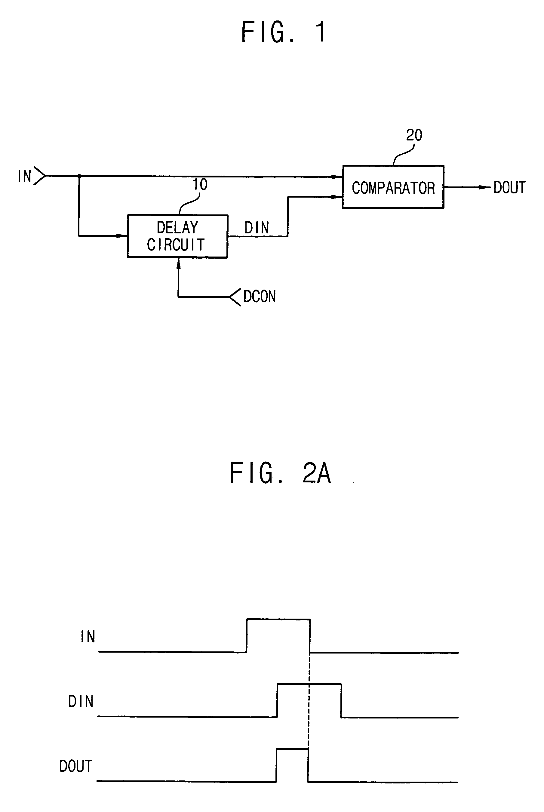
[0059]FIG. 1 is a block diagram illustrating a circuit for describing a method of detecting a delay time according to an exemplary embodiment of the present invention. The circuit of FIG. 1 includes a delay circuit 10 and a comparator 20.

[0060]The delay circuit 10 receives an input signal IN, and delays the input signal IN by a predetermined time to generate a delayed input signal DIN under the control of a delay control signal DCON. The comparator 20 generates an output signal DOUT in response to the input signal IN and the delayed input signal DIN.

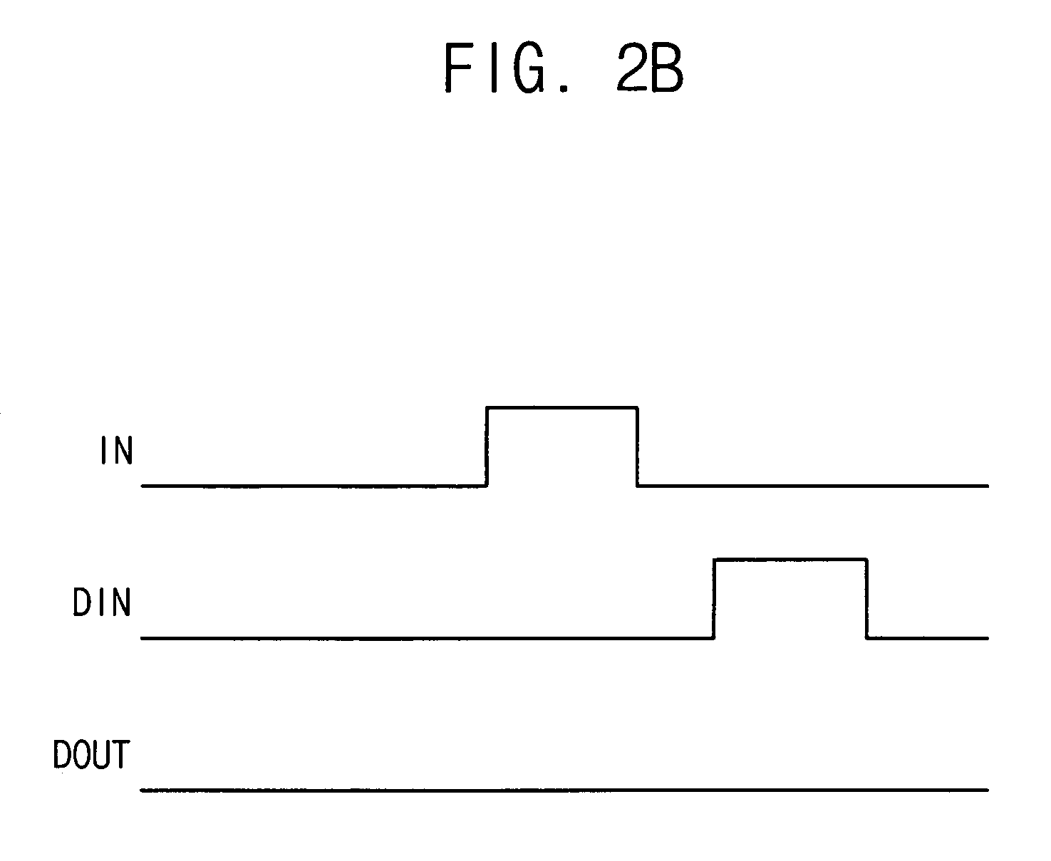
[0061]FIG. 2A and FIG. 2B are timing diagrams illustrating the operation of the circuit of FIG. 1.

[0062]Hereinafter, a method of detec...


PUM


Abstract

A delay control circuit capable of controlling a delay time is disclosed. The delay control circuit includes a delay detecting circuit, a first pulse generator, a counter control circuit and a counter. The delay detecting circuit delays an input signal by a first time in response to an output signal and compares the input signal and the delayed input signal to generate a first signal. The first pulse generator generates a second signal in response to the input signal. The counter control circuit generates a count-up signal and a count-down signal in response to the first signal and the second signal. The counter generates the output signal in response to the count-up signal and the count-down signal to divide the first time by 2n intervals, wherein n is a positive integer.

Description

CROSS-REFERENCE TO RELATED APPLICATION[0001]This application claims priority under 35 U.S.C. § 119 to Korean Patent Application No. 2005-3643, filed on Jan. 14, 2005, the disclosure of which is incorporated by reference herein in its entirety.BACKGROUND OF THE INVENTION[0002]1. Technical Field[0003]The present invention relates to a delay control circuit and a method of controlling a delay of a semiconductor device, and more particularly, to a circuit and a method, which detect and control a delay time in accordance with a change in operating conditions of the semiconductor device.[0004]2. Discussion of the Related Art[0005]A delay time of a delay circuit in a semiconductor device typically changes according to operating conditions affecting the semiconductor device. In particular, operating conditions such as a fabrication process, temperature, and voltage may change of the delay time and thus affect the operation of the semiconductor device.[0006]For example, when the delay time i...

Claims


Application Information

Patent Timeline
Patent Type & Authority Patents(United States)
IPC IPC(8): H03H11/26G06F1/06H03K5/13H03K5/26
CPCH03K3/35625H03K5/26H03K5/133H03L7/0814H03K2005/00065H03K2005/00293H03K2005/00247G11C8/00
Inventor JUNG, HYUN-TAEK
Owner SAMSUNG ELECTRONICS CO LTD
Learn More