Semiconductor device and manufacturing method thereof

a technology applied in the field of semiconductor chips and manufacturing methods, can solve the problems of reducing the yield of chips, weak connection, and difficulty in reducing the size of the device, and achieve the effects of reducing the restriction on combinations of semiconductor chips, reducing the package size, and reducing the restriction on the number of semiconductor chips

Inactive Publication Date: 2007-10-02
SAMSUNG ELECTRONICS CO LTD
View PDF20 Cites 11 Cited by
  • Summary
  • Abstract
  • Description
  • Claims
  • Application Information

AI Technical Summary

Benefits of technology

[0015]An object of the present invention is to provide a semiconductor device which is capable of reducing a package size and providing a sufficient clearance between wires and reducing restrictions on combinations of semiconductor chips to be stacked, and to provide a manufacturing method of such a semiconductor device.
[0018]With the above method and arrangement, the wire bonding of the two different layers of the multiple layers composed of the substrate and the semiconductor chips are carried out by the reverse method by which the wire is provided from the bonding pad on the bottom layer to the bonding pad on the upper layer. Thus, compared with the forward method in which the wire is provided in the reversed direction (order) from the reverse method, bonding can be made stably by suppressing the wire height even when the wire length is long. Further, because the wire rises straight up almost perpendicular to the first bonding portion, a clearance between wires can easily be provided. Also, even though the capillary needs to be moved in a direction away from the semiconductor chip in first bonding to flex the wire in the form of a shoulder, because there is no semiconductor chip (upper layer) is provided in this direction, the bonding pads on the substrate (lower layer) can be disposed close to one another.
[0019]Further, in second bonding on the semiconductor chip, the capillary moves perpendicularly without flowing in a direction toward the semiconductor chip of the adjacent upper layer, and thus the clearance between the bonding pad of the semiconductor chip to be subjected to second bonding and the edge of the semiconductor chip of the adjacent upper layer can be reduced, thus reducing restrictions on combinations of semiconductor chips to be stacked.
[0020]Thus, by using the reverse method in the ball bonding method to connect the stacked semiconductor chips and the substrate, it is possible to reduce the package size and to provide a sufficient clearance between wires and also to reduce restrictions on combinations of semiconductor chips to be stacked.

Problems solved by technology

Also, in the wedge bonding method, when the semiconductor chip of the upper layer is small, it is required to position a bonding pad on the substrate away from an end of the semiconductor chip of the bottom layer because it is difficult to flex the wire.
Further, because the aluminium wire used in wedge bonding is crushed to make the connection, if the wire is jiggled up and down after first bonding to change the shape of the wire loop, the connection becomes weak.
Thus, in the reverse method of the wedge bonding method, it is difficult to bend the wire at an angle near the right angle, and the wire takes a circular shape with a round shoulder, thus making it difficult to reduce the size of the device.
Also, when the semiconductor chips 2 and 3 of the upper layers are increased in size to reduce the distance Lc, the yield of the chips is reduced, making the method unsuitable.
As described, the conventional wire bonding method adopting the forward method has the problem that many restrictions are imposed on combinations of semiconductor chips to be stacked in wire bonding of the multi-layered semiconductor device.

Method used


Image

  • Semiconductor device and manufacturing method thereof
  • Semiconductor device and manufacturing method thereof
  • Semiconductor device and manufacturing method thereof

Examples


Embodiment Construction

[0038]The following will describe one embodiment of the present invention referring to FIG. 1 through FIG. 8.

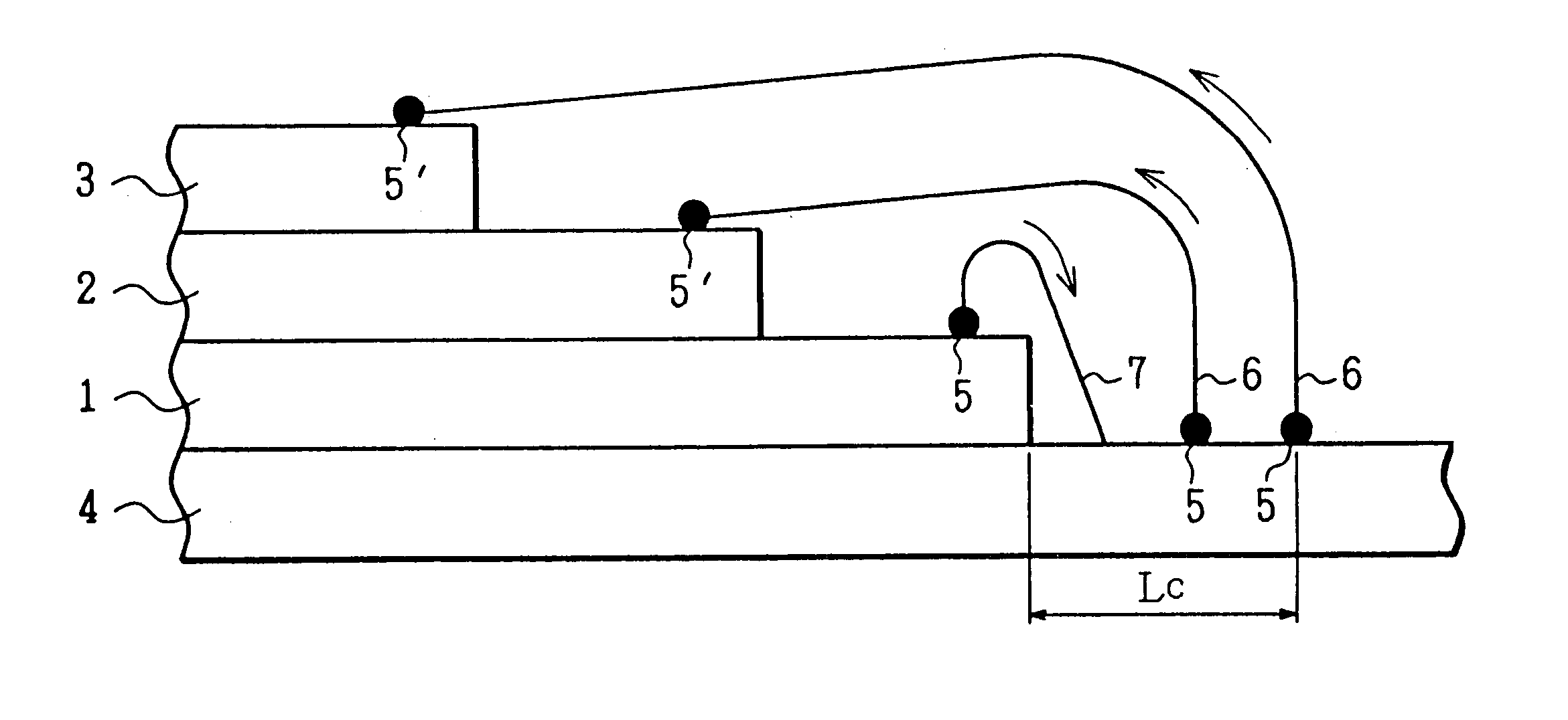
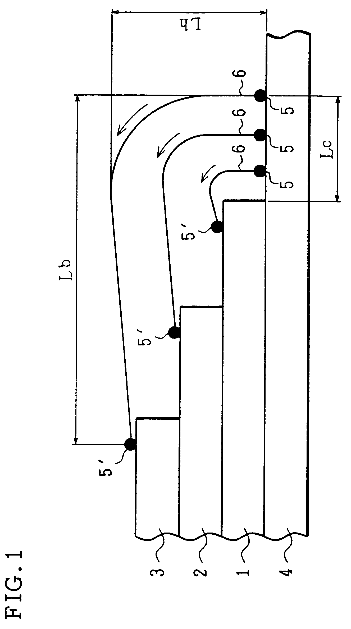
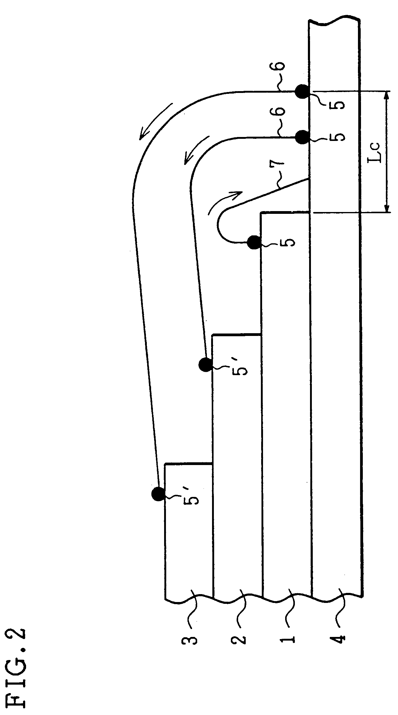
[0039]As shown in FIG. 1, a semiconductor device in accordance with the present embodiment is a multi-layered semiconductor device having a three-layered structure in which a semiconductor chip 1 as a first layer, semiconductor chip 2 as a second layer, and semiconductor chip 3 as a third layer are stacked on a substrate 4 in this order, and the bonding pads of the semiconductor layers and the substrate are connected to each other by a ball bonding method.

[0040]Specifically, the connection is made by melting the tip of gold wire 6 which has been led through a capillary (bonding capillary) to form a ball, and by press-bonding the ball with heat on each bonding pad of the semiconductor chips 1 to 3 and the substrate 4. Note that, the wire bonding is made from the bottom layer. Also, the wire is not limited to the gold wire and other wires such as a copper wire may also be used....


PUM


Abstract

In a manufacturing method of a semiconductor device, a substrate and a plurality of semiconductor chips stacked on the substrate are connected to each other by a ball bonding method adopting a reverse method. Specifically, after first bonding on a bonding pad on the substrate, a gold wire is led to a bonding pad of a semiconductor chip of the bottom layer, and by second bonding, a wire for connecting the substrate and the semiconductor chip of the bottom layer is formed. Similarly, other semiconductor chips are also connected to the substrate from the layer on the bottom. As a result, it is possible to reduce the package size, to provide a sufficient clearance between wires, and to reduce restrictions on combinations of semiconductor chips to be stacked.

Description

[0001]This application is a Divisional of application Ser. No. 10 / 162,864, filed Jun. 6, 2002 (abandoned), which is a Divisional of Ser. No. 09 / 495,300, filed Feb. 1, 2000 (abandoned), the entire contents of which are incorporated herein by reference in this application.FIELD OF THE INVENTION[0002]The present invention relates to a semiconductor device to be used in a stacked package in which a plurality of semiconductor chips are stacked, and to a manufacturing method thereof.BACKGROUND OF THE INVENTION[0003]A stacked package, in which a plurality of semiconductor chips are stacked, is one solution for the demand of smaller, lighter, and higher functioning electric devices including portable devices.[0004]In assembling the stacked package, as the wire bonding method for making an electrical connection between the semiconductor chips and the substrate, a ball bonding (nail-head bonding) method using a gold wire, or a wedge bonding method using an aluminium wire is adopted.[0005]In t...

Claims


Application Information

Patent Timeline
Patent Type & Authority Patents(United States)
IPC IPC(8): H01L21/44H01L25/18H01L21/60H01L25/00H01L25/04H01L25/065H01L25/07
CPCH01L24/49H01L24/85H01L25/0657H01L25/50H01L24/48H01L24/45H01L2924/12041H01L24/78H01L2224/32145H01L2224/32225H01L2224/45144H01L2224/45147H01L2224/4809H01L2224/48091H01L2224/48095H01L2224/48137H01L2224/48145H01L2224/48147H01L2224/48227H01L2224/48464H01L2224/48465H01L2224/48471H01L2224/48475H01L2224/48479H01L2224/48599H01L2224/49052H01L2224/4911H01L2224/4942H01L2224/49425H01L2224/49429H01L2224/4945H01L2224/73265H01L2224/78301H01L2224/85051H01L2224/85181H01L2224/85186H01L2224/85191H01L2224/85951H01L2225/06506H01L2225/0651H01L2225/06555H01L2924/01004H01L2924/01005H01L2924/01006H01L2924/01013H01L2924/01015H01L2924/01029H01L2924/01057H01L2924/01079H01L2924/01082H01L2924/014H01L2924/15311H01L2924/30105H01L2924/01033H01L2224/45124H01L2224/05553H01L2224/85203H01L24/73H01L2224/48499H01L2924/181H01L2224/05644H01L2924/00014H01L2924/00H01L2924/00012H01L2924/00015H01L2224/4554A63B53/14A63B53/08A63B60/06A63B2102/32
Inventor YANO, YUJINARAI, ATSUYA
Owner SAMSUNG ELECTRONICS CO LTD
Why Eureka
Try Eureka