Pixel design including in-pixel correlated double sampling circuit

a double sampling circuit and pixel design technology, applied in the field of image sensor array configuration, can solve the problems of increasing reset noise, cmos imagers have typically higher noise than ccd imagers, and the operation of most cmos imagers does not allow true cds, so as to achieve the effect of reducing pixel reset noise and feedthrough error, reducing cost and chip area, and effectively implementing

Inactive Publication Date: 2007-10-02
SMAL CAMERA TECH
View PDF23 Cites 49 Cited by
  • Summary
  • Abstract
  • Description
  • Claims
  • Application Information

AI Technical Summary

Benefits of technology

[0006]With this pixel and image sensor configuration, pixel reset noise and feedthrough error are significantly reduced from that typical of conventional pixel designs. In addition, the pixel sample and hold circuit of the invention enables the storage of a pixel output voltage at that pixel for subsequent correlated double sampling operations; no external storage capacity is required. Further, because the invention does not require the use of an amplifier at each pixel, instead providing for column-wise or row-wise sharing of a single amplifier, cost and chip area are minimized; the amplifier can be connected to accept an output signal from a pixel selected from a column of pixels or selected from a row of pixels. As a result, correlated double sampling of pixel outputs from pixel arrays, such as CMOS pixel arrays, can be efficiently and effectively implemented in a manner not previously attainable.
[0007]In implementations of the pixel sample and hold circuit of the invention, each pixel can be provided with a second select node that is connected to receive a second select signal for coupling the output signal of the amplifier to the sample and hold circuit of that pixel. A coupling capacitor can be provided in a connection to couple the incident light intensity signal at the sense node with the sample and hold circuit. In one example, this coupling capacitor is connected to a sample and hold storage capacitor in a voltage divider configuration that enables attenuation of pixel reset noise and pixel feedthrough error. Such can be particularly advantageously implemented with a storage capacitor capacitance that is at least about an order of magnitude less than the capacitance of the pixel coupling capacitor.

Problems solved by technology

However, CMOS imagers have typically higher noise than CCD imagers.
While CCD imagers employ correlated double-sampling (CDS) to remove the reset noise commonly referred to as kTC noise, the operation of most CMOS imagers does not allow for true CDS.
Unfortunately, this method often actually increases reset noise.
In particular, the inclusion of a separate amplifier in each pixel substantially increases the size and cost of an imaging array of such pixels.
As a result, a tradeoff between CDS functionality and imager array size and cost has typically been required.

Method used


Image

  • Pixel design including in-pixel correlated double sampling circuit
  • Pixel design including in-pixel correlated double sampling circuit
  • Pixel design including in-pixel correlated double sampling circuit

Examples


Embodiment Construction

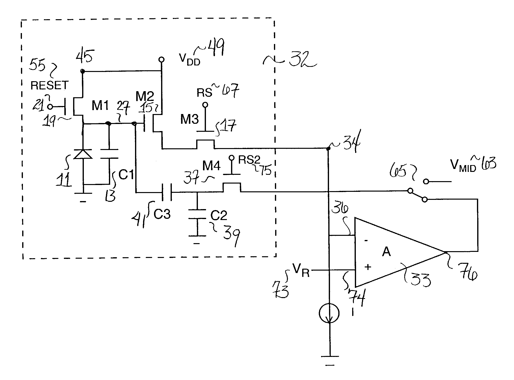
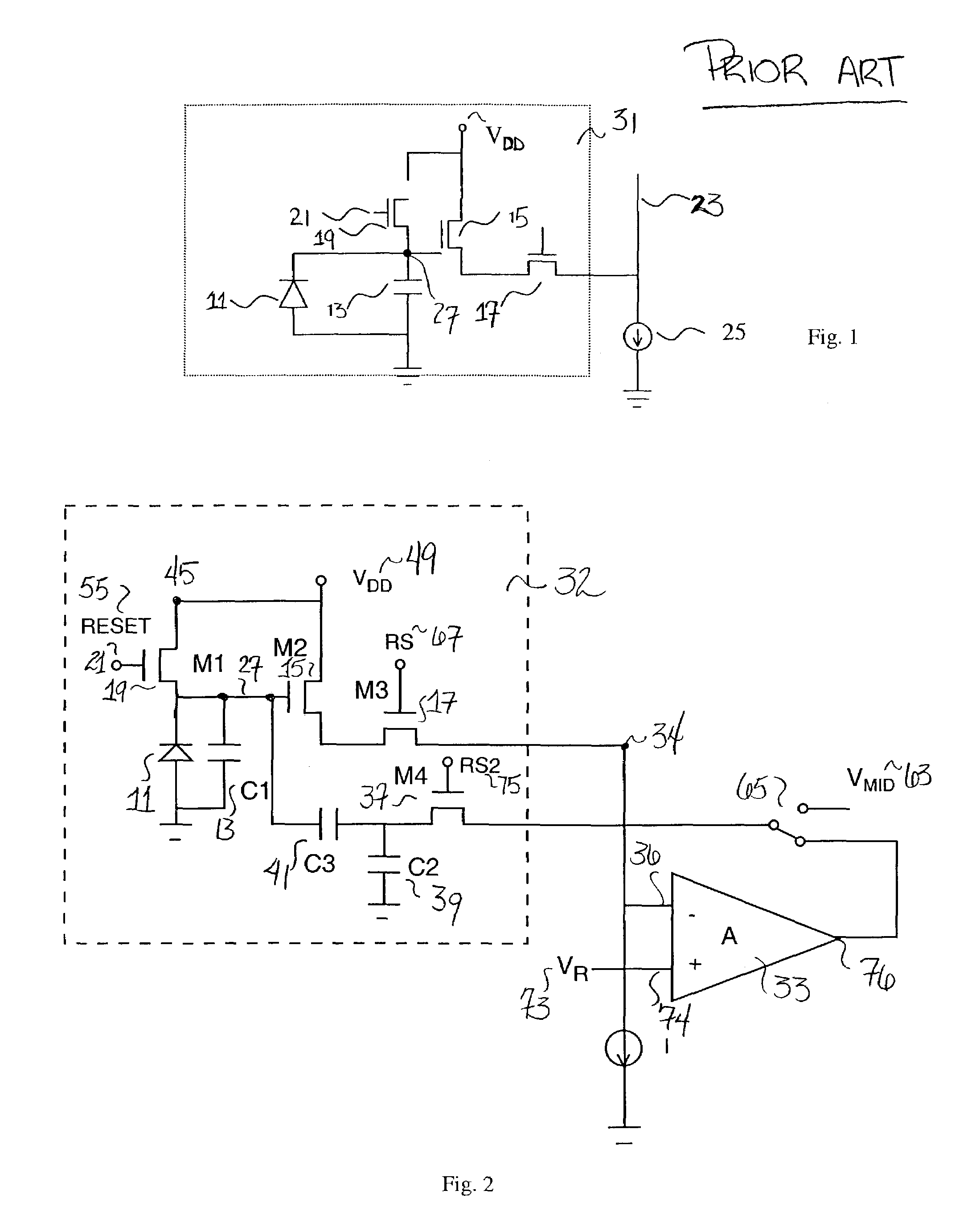
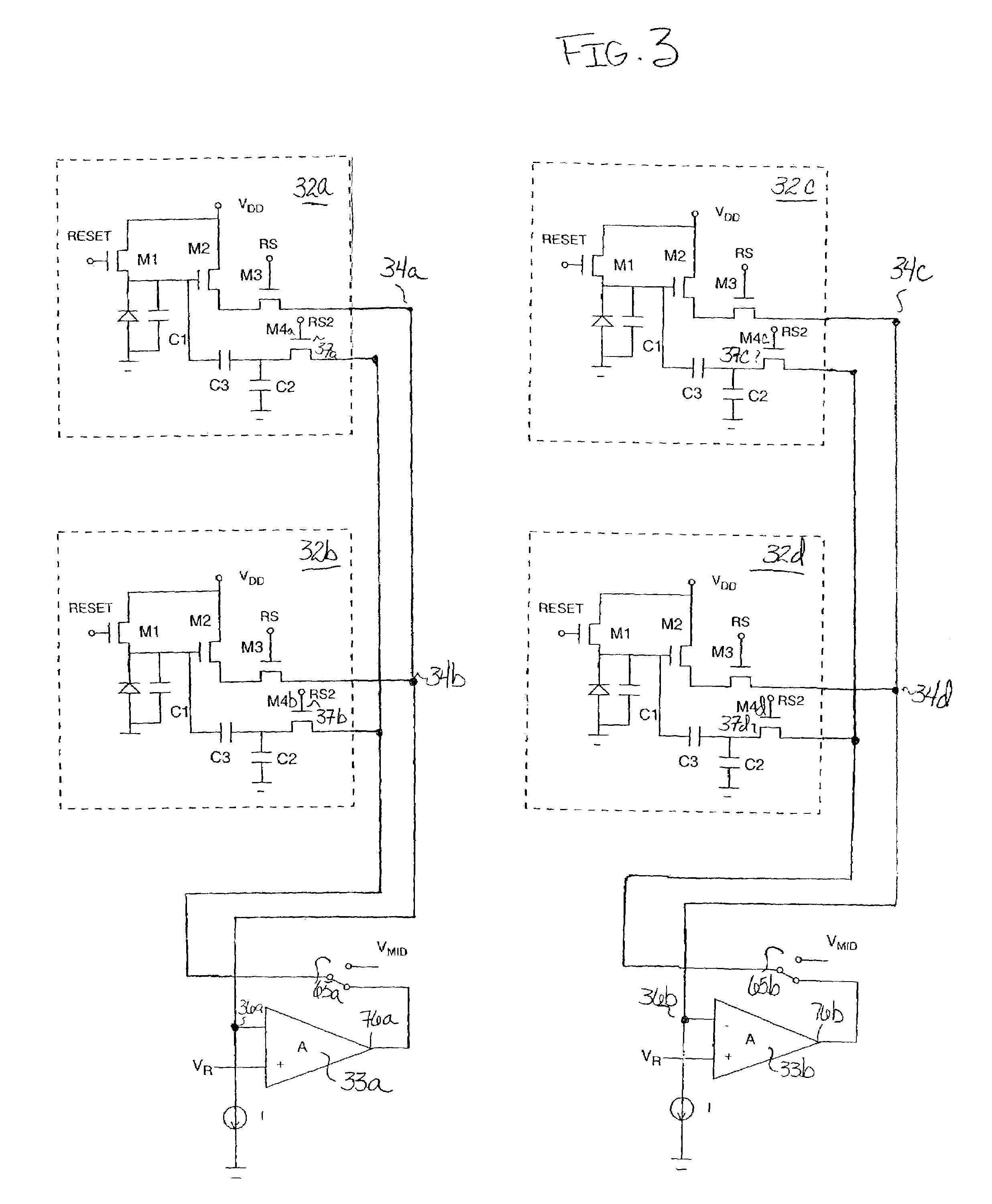
[0017]FIG. 1 is a schematic diagram of a conventional CMOS active pixel 31. A first device or circuit, for example, a photocircuit such as a photodiode 11, produces a current proportional to the incident light intensity on the pixel. The photocircuit could alternatively produce a proportional voltage or charge. The resulting, e.g., photocurrent, is integrated on a charge sensing capacitor 13. The charge-sensing capacitor 13 may be any source of capacitance, but is typically preferably provided by the parasitic reverse-biased PN junction capacitance associated with the photodiode 11 and other devices in the pixel. During a defined pixel charging period, a row select MOS switch transistor 17 and a MOS reset transistor 19 are both maintained “off.”

[0018]Then, at the end of a pixel integration period, when a particular row of such pixels in an imager array of pixels is selected for read-out of pixel values, the row select MOS switch transistor 17 is turned “on” to activate a source foll...


PUM


Abstract

An image sensor having a plurality of pixels, each including a sense node; an output node; a first device, connected to the sense node, producing a signal at the sense node that is proportional to incident light intensity at the pixel; at least one select node to receive a first select signal for selecting the pixel output node from the plurality of pixels; a reset device for resetting the pixel; and a sample and hold circuit including a sample node coupled to the sense node. At least one amplifier is provided, including a first input node to receive an output signal from the output node of a selected pixel and a second input node connected to a reference voltage source provided as a reference to reset a selected pixel. An amplifier output node is connected to couple an amplifier output signal to a selected pixel's sample and hold circuit.

Description

BACKGROUND OF INVENTION[0001]This invention relates to image sensor array configurations for reducing image array pixel reset noise. More specifically, the invention relates to pixel designs for resetting pixels in a manner that reduces pixel reset noise.[0002]CMOS image sensors are attractive due to the compatibility with VLSI circuits. However, CMOS imagers have typically higher noise than CCD imagers. While CCD imagers employ correlated double-sampling (CDS) to remove the reset noise commonly referred to as kTC noise, the operation of most CMOS imagers does not allow for true CDS. Instead, uncorrelated double-sampling is typically employed to remove the constant reset level. Unfortunately, this method often actually increases reset noise.[0003]There have been proposed various CMOS pixel designs that incorporate correlated-doubling sampling functionality in the pixel itself. Although such circuits are found to often substantially remove the reset noise, in general such designs req...

Claims


Application Information

Patent Timeline
Patent Type & Authority Patents(United States)
IPC IPC(8): H04N3/14H01L27/00H04N5/217H04N5/335H04N5/363H04N5/374H04N5/378
CPCH04N5/357H04N5/378H04N5/37452H04N5/3575H04N25/60H04N25/616H04N25/771H04N25/75
Inventor LEE, HAE-SEUNG
Owner SMAL CAMERA TECH
Why Eureka
Try Eureka